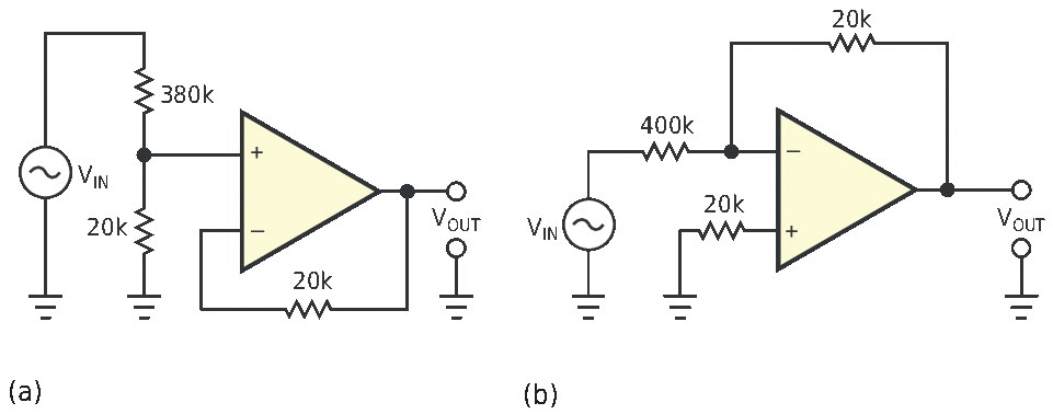
Figure 1 shows two large-signal- measurement methods. The first uses a two-resistor voltage divider and an output buffer, and the second comprises an attenuating inverter and a high-value input resistor. Both of these approaches introduce measurement-linearity errors because only a single resistor dissipates power, which leads to self-heating and its associated change in resistance. In addition, the amplifier and the remaining resistors introduce a combination of offset current, offset voltage, CMRR (common-mode-rejection-ratio) effects, gain error, and drift, which may significantly reduce the system's overall performance.
 |
|
| Figure 1. | To measure high voltages, you can use discrete resistors to assemble an input voltage divider and buffer (a) or an attenuating inverter (b), but performance suffers due to thermal mismatch. |
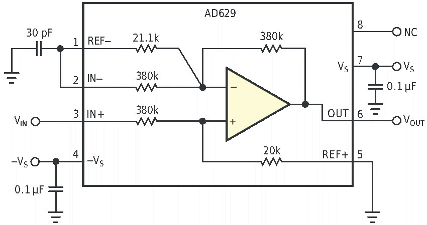
Based on Analog Devices' AD629, the circuit in Figure 2 can measure inputs in excess of 400 V p-p with less than 5-ppm linearity error. The circuit attenuates its input signal by a factor of 20 and delivers a buffered output. Packaging the amplifier and attenuator resistors together ensures that both resistors in the attenuator string operate at the same temperature. The amplifier's input stage employs superbeta transistors to minimize offset current and errors due to bias current errors. Applying 100% feedback at low frequencies introduces no noise gain, and the offset voltage and its drift add almost no error.
 |
|
| Figure 2. | An integrated approach moves external resistors into the device’s package for improved thermal tracking and greater accuracy. |
The AD629 is unstable with 100% feedback, and the 30-pF capacitor adds a pole and a zero to the feedback gain to stabilize the circuit and maximize the system bandwidth.
The following equation calculates the pole frequency, fP:

The following equation determines the zero frequency, fZ:

 |
|
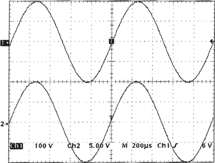
| Figure 3. | The circuit in Figure 2 delivers a 20 V p-p output for a 400 V p-p input. |
 |
|
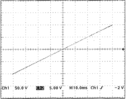
| Figure 4. | Plotting input versus output shows minimal departure from an ideal straight line for a 400 V p-p input. |
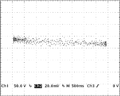
Figure 3 shows the amplifier's performance with a 400 V p-p input (upper trace) and its corresponding 20 V output (lower trace). In Figure 4, a cross plot shows linearity for a 50 V/division input signal and a 5 V/division output. Figure 5, a linearity-error plot, shows nonlinearity versus a 400 V p-p input signal.
 |
|
| Figure 5. | A scatter plot of nonlinearity error for a 400 V p-p input displays error of less than 10 ppm over the input range. |