The gain temperature coefficient of conventional V-F circuits is affected by drift in the charge pumping capacitors. Although compensation schemes are employed to minimize the effect of this drift, another approach is required to get significantly lower gain drift.
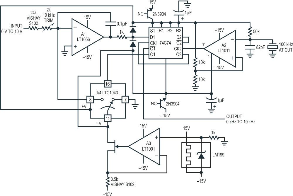
Figure 1’s circuit reduces gain TC to 5 ppm/°C by replacing the capacitor with a quartz-stabilized clock.
 |
|
| Figure 1. | Quartz-stabilized V-F. |
In charge pump-based circuits the feedback is based on Q = CV. In a quartz-stabilized circuit the feedback is based on Q = IT, where I is a stable current source and T is an interval of time derived from the clock.
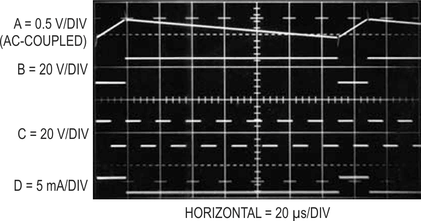
Figure 2 details Figure 1’s waveforms of operation. A positive input voltage causes A1 to integrate in the negative direction (Trace A, Figure 2). The flip-flop’s Q1 output (Trace B) changes state at the first positive-going clock edge after A1’s output has crossed the D input’s switching threshold. The 50 kHz clock (Trace C) comes from the flip-flop’s other half, which is driven by A2, a quartz-stabilized relaxation oscillator. The flip-flop’s Q1 output controls the gating of a precision current sink composed of A3, the LM199 voltage reference, a FET and the LTC1043 switch. When A1 is integrating negative, the Q1 output is high and the LTC1043 directs the current sink’s output to ground via Pins 11 and 7. When A1’s output crosses the D input’s switching threshold, Q1 goes low at the first positive clock edge. LTC1043 Pins 11 and 8 close and a precise, quickly rising current flows out of A1’s summing point (Trace D).
 |
|
| Figure 2. | Waveforms for quartz-stabilized V-F. |
This current, scaled to be greater than the maximum signal- derived input current, causes A1’s output to reverse direction. At the first positive clock pulse after A1’s output crosses the D input’s trip point, switching again occurs and the entire process repeats. The repetition frequency depends on the input-derived current, hence the frequency of oscillation is directly related to the input voltage. The circuit’s output may be taken from the flip-flop’s Q1 or /Q1 outputs. Because this circuit replaces the capacitor with a quartz-locked clock, temperature drift is low, typically 5 ppm/°C. The quartz crystal contributes about 0.5 ppm/°C, with the remaining drift a function of the current source components, switching time variations and the input resistor.
The reverse-biased 2N3904s serve as Zener diodes, providing about 15 V across the CMOS flip-flop. The diodes at the D1 input prevent transient overdrive from A1 during circuit start-up.
A V→F of this type is usually restricted to relatively low full-scale frequencies, e.g., 10 kHz to 100 kHz, because of speed limitations in accurately switching the current sink. Additionally, short-term frequency jitter may occur because of the uncertain timing relationship between A1’s output switching the flip-flop and the clock phase. This is normally not a problem because the circuit’s output is usually read over many cycles, e.g., 0.1 to 1 second.
As shown circuit linearity is 0.005%, gain temperature coefficient is 5 ppm/°C and full-scale frequency is 10 kHz. The LT1056’s low input offset reduces zero point error to 0.005 Hz/°C. To trim this circuit, apply exactly 10 V in and adjust the 2k potentiometer for 10.000 kHz output.