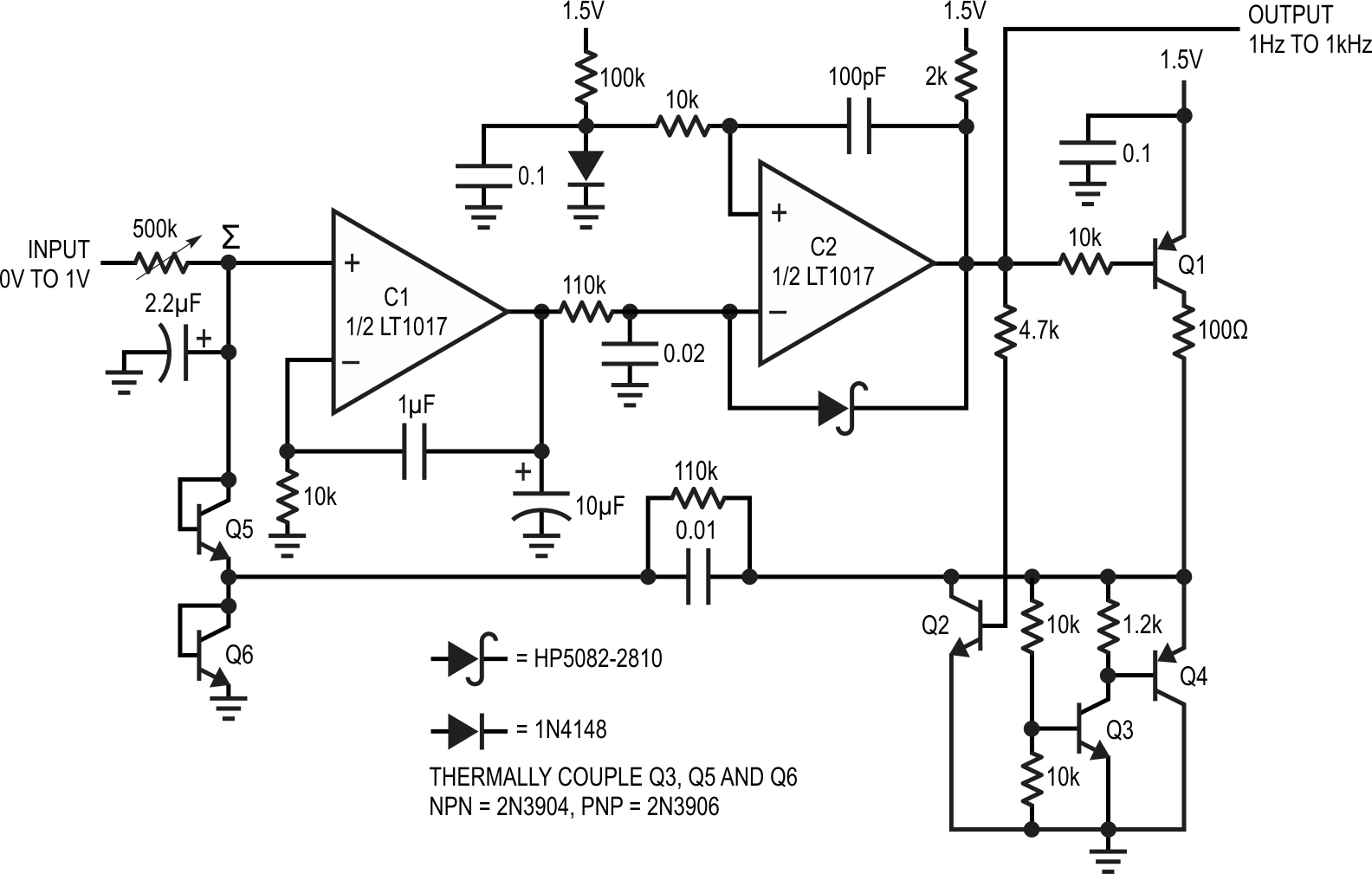
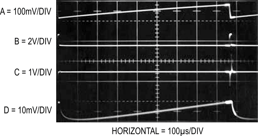
High speed and precision are not the only areas where special V-F circuits are needed. Figure 1 shows a circuit which runs from a single 1.5 V cell with only 125 µA current drain. The circuit uses an LT1017 dual micropower comparator in a servo-controlled charge pump configuration. The input is applied to C1, which is compensated by the 10 µF and 1 µF capacitors to act as an op amp. C1’s output drives the 110k-0.02 µF RC, causing the capacitor to ramp (Trace A, Figure 2).
 |
|
| Figure 1. | Single cell V-F. |
During the ramp, C2’s output is high, turning off Q1 and biasing Q2 on. The potential across the Q3-Q4 VBE voltage reference (Trace B) is zero. The 0.01 µF capacitor receives no charge. When the ramp equals the potential at C2’s positive input, switching occurs. C2’s output goes low, and the 0.02 µF unit discharges. AC positive feedback (Trace C) “hangs up” C2 long enough for a ramp reset of about 80 mV. Concurrently, Q1 comes on and Q2 goes off. The Q3-Q4 reference comes on (Trace B) and charges the 0.01 µF capacitor via Q6.
 |
|
| Figure 2. | Single cell V-F waveforms. |
When the positive feedback at C2 ceases, its output returns high, cutting off Q1 and biasing Q2. Now, the 0.01 µF capacitor discharges, forcing current to flow from C1’s 2.2 µF summing point capacitor (Trace D) via Q5 and Q2. C1 servo-controls this oscillator to whatever frequency is required to maintain C1’s summing point near zero. Since the current into C1’s input is a linear function of the input voltage, oscillator frequency is also linear. The 1 µF-10k combination at C1 provides loop stability. The 110k resistor across the 0.01 µF capacitor influences its discharge characteristic, aiding overall circuit linearity.
The temperature coefficient of the 1.2 V Q3-Q4 reference is largely compensated by the junction tempcos of Q5 and Q6, giving the circuit a 250 ppm/°C gain drift. Battery discharge introduces less than 1% error over 1000 hours operation.