An excerpt from Christopher Paul’s “Parsing PWM (DAC) performance: Part 1 – Mitigating errors” (Ref. 1):
“I was surprised to discover that when an output of a popular µP I’ve been using is configured to be a constant logic low or high and is loaded only by a 10 MΩ-input digital multimeter, the voltage levels are in some cases more than 100 mV from supply voltage VDD and ground… Let’s call this saturation errors.”
The accuracy of PWM DACs depends on several factors, but none is more important than their analog switching elements’ ability to reliably and precisely output zero and reference voltage levels in response to the corresponding digital states. Sometimes however, as Christopher Paul observes in the cited design idea (Part 1 of a 4-part series), they don’t. The mechanism behind these deviations isn’t entirely clear, but if they could be reliably eradicated, the impact on PWM performance would have to be positive. Figure 1 suggests a (literally) brute-force fix.
 |
|
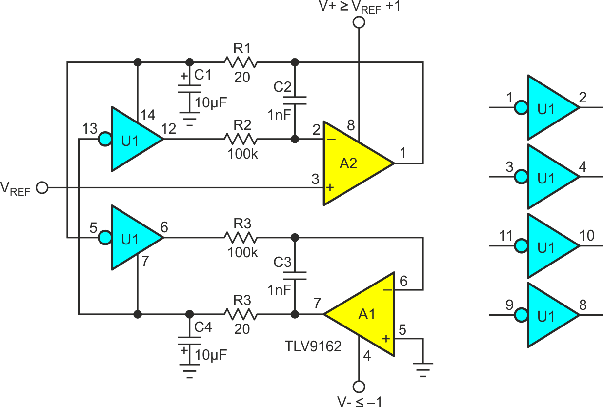
| Figure 1. | U1 is a multi-pole (e.g., 74AC04 hex inverter) PMW switch where op-amp A1 forces switch zero state to accurately track 0 = zero volts, op-amp A2 does the job for 1 = VDD. |
U1 pin 5’s connection to pin 14 drives pin 6 to logic 0, sensed by A1 pin 6. A1 pin 7’s connection to U1 pin 7 forces the pin 6 voltage to exactly zero volts, and thereby forces any U1 output to the same accurate zero level when the associated switch is at logic 0.
Similarly, U1 pin 13’s connection to pin 7 drives pin 12 to logic 1, sensed by A2 pin 2. A2 pin 1’s connection to U1 pin 14 forces the pin 12 voltage to exactly VDD, and thereby forces any U1 output to the same accurate VREF level when the associated switch is at logic 1.
Thus, any extant “saturation errors” are forced to zero, regardless of the details of where they’re actually coming from.
VDD will typically be c.a. 5.00 V. And V+ and V- can come from a single 5-V supply via any of a number of discrete or monolithic rail boost circuits. Figure 2 is one practical possibility.
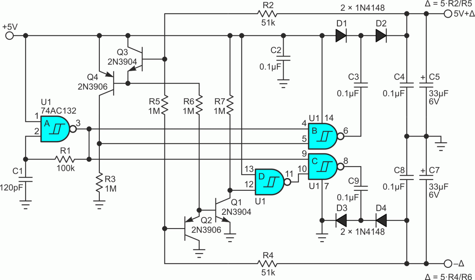 |
|
| Figure 2. | A practical source for V+ and V- set R1 and R2 = 200k for ∆ = 1 volt. |
The Figure 2 circuit was originally described in “Efficient digitally regulated bipolar voltage rail booster” (Ref. 2).
References
- Paul, Christopher. ”Parsing PWM (DAC) performance: Part 1 – Mitigating errors.”
- Woodward, Stephen. “Efficient digitally regulated bipolar voltage rail booster.”