Analog-to-digital conversion based on the classic combination of a voltage-to-frequency converter (VFC) with a counter has been around for (many) decades, mainly because it has some durable time-proven advantages. VFC digitization is naturally integrating, so high noise rejection is inherent, as is programmable resolution (if you want more bits, just count longer). Unfortunately, high conversion speed is not.
Useful resolution (8 or more bits) tens-of-microseconds VFC conversion times require tens-of-megahertz output frequencies. There are existing VFC designs that can flap that fast, e.g., Jim Williams’s awesome 100 MHz King Kong (Reference 1) and my own “20 MHz VFC with take-back-half charge pump” (Reference 2). However, these possible solutions only pose another potentially pesky problem. What to use for a counter?
Frequently (no pun intended) the ideal and most cost-effective digital partner for a VFC is the µC’s onboard counter-timer peripheral (CTP), typically providing 16 bits of resolution at zero added parts cost. Unfortunately, the necessity of taking multiple (e.g., four) samples of each cycle of incoming pulses by onboard CTP logic limits maximum count rate to a fraction (typically ¼) of the µC’s internal clock.
Thus, for a 20-MHz internal clock, 5 MHz is the fastest achievable CTP count rate. Sorry, Kong.
Of course, an external hardwired counter peripheral could be implemented that would easily accommodate fast VFCs (okay, maybe Kong not so totally easy), but cost, parts count, and board area make this option quite unattractive.
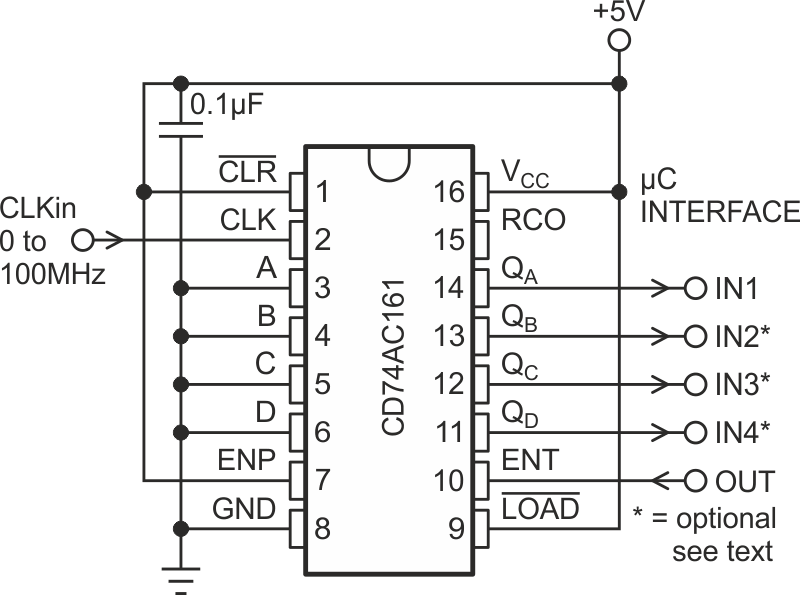
Shown in Figure 1 is a compromise topology that combines the CTP doing what it does best (providing lots of bits), with a single external 4-bit MSI pre/scaler/accumulator chip. This extends the peripheral’s speed by up to 16x (hence up to 80 MHz with a CTP 5-MHz top end), at the cost of (at most) four additional general purpose I/O (GPIO) pins.
 |
|
| Figure 1. | 100-MHz MSI counter prescales and accumulates VFC LSBs so clunky CTP can cope. |
Here’s how it works.
- Five GPIO pins are programmed for interface with the preaccumulator:
a. Four as inputs (IN1 through IN4),
b. One as output (OUT). - IN4 is also programmed for input to the selected CTP, which is programmed for 16-bit accumulation.
Each VFC integration cycle comprises the following steps:
- OUT = 0 to disable counting.
- A 20-bit initial value (X1) is formed by concatenating the states of the INx bits (as 4 LSBs) with the 16 bits of the CTP (as 16 MSBs), i.e., X1 = [cccc cccc cccc cccc iiii].
- OUT = 1 for the desired integration interval. A practical maximum = 220/VFCmax, shorter if lower resolution and/or higher conversion speed is required.
- OUT = 0 to freeze counting.
- A 20-bit final value (X2) is formed by concatenating INx with the CTP.
- The 20-bit conversion result = X2 – X1 modulo 220.
Note that if the ratio of max VFC output to max CTP count rate is less than 8x, then only three INx pins need be allocated to the interface (Xx = [ccc cccc cccc ciii]), with IN3 programmed as CTP input. If less than 4x, then only two, (Xx = [cc cccc cccc ccii]). And so forth.
If simpler arithmetic is more important than conserving GPIO pins, then a sixth output pin can be connected to /LOAD and pulsed low at the onset of conversion to reset the INx bits to zero, along with a similar preload of the CTP bits. This would eliminate steps #6 and #10 of the conversion sequence.
References
- Williams, Jim. "Designs for High Performance Voltage-to-Frequency Converters."
- Woodward Stephen. "20 MHz VFC with take-back-half charge pump."