A variety of analog front-end functions typically assist ADCs to do their jobs. These include instrumentation amplifiers (INA), digitally programmable gain (DPG), and sample and holds (S&H). The circuit in Figure 1 is a bit atypical in merging all three of these functions into a single topology controlled by the timing from a single (PWM) logic signal.
Figure 1’s differential INA style input starts off conventionally, consisting of tera-ohm impedance and picoamp bias CMOS followers U1a and U1b. The 916x family op-amps are pretty good RRIO devices for this job, with sub-mV input offset, 110 dB CMR, 11 MHz gain-bandwidth, 33 V/µs slew rate, and sub-microsecond setting time. They’re also inexpensive. Turning this into a high CMR differential input, however, is where the circuit starts to get unconventional. The ploy in play is the “flying capacitor”.
 |
|
| Figure 1. | Two generic chips and five passives make a versatile and unconventional ADC front end. |
During the logic-0 interval of the PWM, through switches U2a and U2b both ends of capacitor C are driven by the unity-gain follower amplifiers with CMR limited only by the amplifier’s 110 dB = 300,000:1. Unlike a typical precision differential INA input, no critical resistor matching is involved. A minimum duration interval of a microsecond or two is adequate to accurately capture and settle to the input signal. When the PWM input transitions to logic-1, one end of C is grounded (via U2b) while the other becomes the now single-ended input to U1c (via U2a). Then things get even less conventional.
The connection established from U1c’s output to C through U1c and R1 creates positive feedback that causes the voltage captured on C to multiply exponentially with a (negative) time-constant of:
Tc = (R1 + (U2 on resistance)) C = (14.3 kΩ + 130) 0.001 µF = 14.43 µs = 10 µs/ln(2).
Due to U1c’s gain = R3/R2 + 1 = 2 the current through R1 from VC:

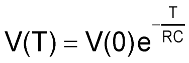
Thus, R1 is made effectively negative which makes R1C negative and for any time T after the 0-1 transition of PWM the familiar exponential decay of:

becomes with a negative R1:

Therefore, taking U1c’s gain of 2.00:

For example, if a 7-bit 1 MHz PWM is used, then each 1 µs increment in the duration of the logic-1 period will equate to a gain increment of 20.1 = 1.072 = 0.60 dB. So, a 100 PWM 1-count would create a gain of

Having 100 available programmable gain settings is a useful and unusual feature.
Note that R1 and C should be precision with low-tempco types like metal film and C0G so that the gain/time relationship will be accurate and stable. The 14.43 µs = 11 kHz roll-off of R1C interacts with the 11 MHz gain bandwidth of U1c to provide ~60 dB of closed loop gain. This is adequate for 10-bit acquisition accuracy.
During this PWM = 1 exponential gain phase, the U2c switch causes the output capacitor and U1d to track VC, which is captured and held for input to the connected ADC during the subsequent PWM = 0 phase. While the front end of the circuit is acquiring the next sample.