A common technique for implementing PWM involves comparing a triangular waveform of fixed amplitude and frequency with a variable dc voltage level. Although this approach results in a PWM signal of precise frequency and with duty cycle variable from 0 to 100%, the need for a reference triangle waveform and a suitable fast comparator can be prohibitively expensive in low-cost applications. Furthermore, if an application requires a high-frequency PWM signal, the power consumption may be unacceptable in power-sensitive applications, such as high-efficiency, low-power switch-mode regulators.
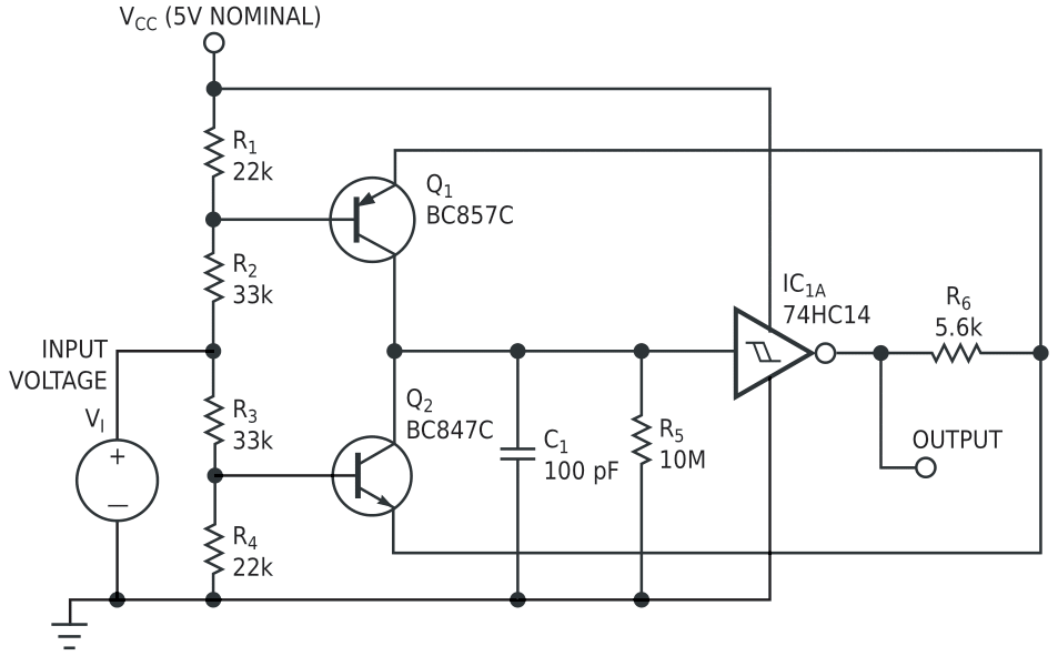
The circuit in Figure 1 is a relatively simple alternative to the triangle/comparator approach. Although the frequency of the output waveform is not stable and varies with input voltage, the circuit is inexpensive, requires only a handful of readily available parts, and exhibits a linear relationship between input voltage and output duty cycle. The circuit lends itself to applications that enclose a simple PWM section within a feedback loop. Also, the excellent dynamics – the duty cycle responds to an input step change within one cycle of the output waveform – make the circuit ideally suited to switch-mode-regulator applications.
In the circuit, the dc input voltage, VI, varies the duty cycle of the rectangular signal at the output of Schmitt inverter, IC1A. Q1 and Q2 function as switched-current sources. These sources charge and discharge timing capacitor C1 at a rate that their base voltages and, hence, the voltage at the junction of R2 and R3 determine. When the output of IC1A is high, C1 charges through R6 and Q1 (Q2 is cut off) with a charge current set by R6 and the emitter voltage of Q1. Similarly, when the output of IC1A is low, C1 discharges via Q2 and R6 (Q1 is cut off) with a discharge current set by R6 and the emitter potential of Q2. Adjusting the input voltage changes the emitter potentials and thus varies the charge and discharge currents so that the duty cycle of the output waveform varies in direct linear proportion to VI.
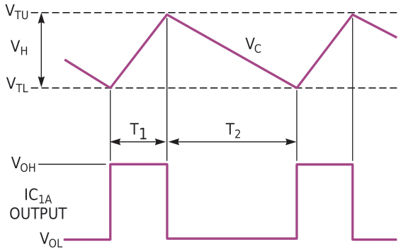
Figure 2 shows the relationship between VC, which is the voltage on C1, and the output waveform. VTU and VTL are the upper and lower thresholds of the Schmitt inverter, VH is the Schmitt trigger's hysteresis, and VOH and VOL are the high and low output levels, respectively, of the inverter.
If you assume that VOH = VCC and VOL = 0 V and taking the base-emitter voltages of Q1 and Q2 to be roughly equal and denoted by VBE, you can derive the following first-order expressions for T1 and T2:

and
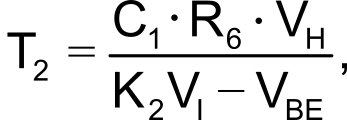
where
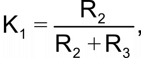
and
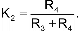
Defining the output duty cycle, D, as equal to 100%×T1/(T1 + T2), you can combine the expression for T1 and T2 to yield

If the R1-to-R4 divider network is symmetrical, or R1 = R4 and R2 = R3, this expression simplifies to

Taking the values for R1 to R4 in Figure 1, the equation reduces to

This expression shows that the duty cycle is directly proportional to the input voltage and that VI must be greater than VBE/0.4 for the circuit to work. If VBE = 0.6 V, this equation suggests that V must be at least 1.5 V, although, in breadboard tests, the circuit produced low duty cycles with VI as low as 1 V.
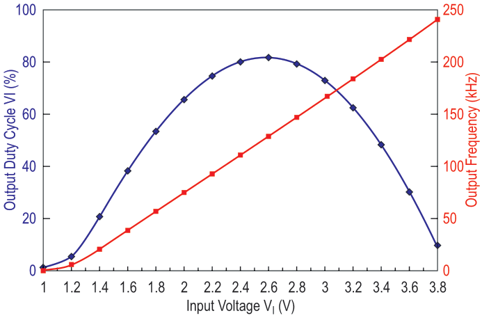
You select C1 and R6 according to the required operating-frequency range. Figure 3 illustrates the results of breadboard tests with R6 = 5.6 kΩ and C1 = 100 pF. The circuit exhibits linear performance with VI at approximately 1.2 to 3.6 V with a corresponding duty-cycle range of approximately 2 to 95%. This figure also shows that the output frequency varies by as much as 15 to 1 over this range; the output frequency peaks when VI is approximately equal to VCC/2.
 |
|
| Figure 3. | Although the frequency of the output waveform varies with the input voltage, the PWM circuit exhibits a linear relationship between input voltage and output duty cycle. |
You need to observe a few caveats when selecting R1 to R4 and IC1A. To ensure that the duty cycle is variable from near zero to near 100%, the charge and discharge currents through Q1 and Q2 must be able to approach zero. You can meet this requirement simply by ensuring that VE1, or Q1’s emitter potential, can approach VCC and that VE2, or Q2’s emitter potential, can approach ground.
You can make VE1 approach VCC when VI is a maximum by the suitable selection of R1 and R2, provided that you choose R3 and R4 so that VE2 can go a few hundred millivolts below the minimum lower threshold voltage, VTL (minimum), of IC1A when VI is a maximum. This feature is necessary to ensure that Q2 does not saturate when VC approaches VTL (minimum) as C1 discharges.
Similarly, by suitably selecting R3 and R4, you can make VE2 approach zero when VI is a minimum, provided that you choose R1 and R2 so that VE1 can go a few hundred millivolts above the maximum upper threshold voltage, VTU (maximum), of IC1A when VI is a minimum. This feature is necessary to ensure that Q1 does not saturate when VC approaches VTU (maximum) as C1 charges.
The values R1 = R4 = 22 kΩ and R2 = R3 = 33 kΩ meet these requirements and provide an optimum range for VI. These values should provide reliable operation for VCC = 5 V±5% and IC1A and IC1A = 74HC14, but you may need to recalculate the values if you use a different supply voltage or a different inverter.
Two possible devices to use for IC1A are the 74HC14 and the 4093. The 74HC14 is preferable because the minimum to maximum variation in its hysteresis voltage is only about 3.3 to 1, whereas the variation in VH for the 4093 is approximately 6.7 to 1. However, the 4093 allows operation at supply voltages greater than 5 V, but take care to avoid base-emitter breakdown of Q1 and Q2 at higher supply voltages.
Power consumption is low. For example, with C1 = 100 pF, the maximum current draw is 570 µA at the point of maximum frequency, which is approximately 200 kHz. The maximum practical operating frequency is limited to around 500 kHz (C1 = 10 pF, R6 = 5.6 kΩ), where the relationship between VI and the duty cycle starts to become noticeably nonlinear.
