As a genre, DACs are low power devices with power and current output capabilities limited to the milliwatt and milliampere range. There is, of course, no fundamental reason they can’t be teamed up with suitable power output stages, which is indeed common practical practice. Problem solved.
But just for fun, this design idea takes a different path to power by merging a venerable (the “L” stands for “legacy!”) LM337 regulator into a simple (just two generic active chips) 8-bit PWM DAC to obtain a robust 1.5-A capability. It also enjoys the inherent overload and thermal protection features of that time-proven Bob Pease masterpiece.
As an extra added zero cost feature, output voltage accuracy is (mostly: ~90%) determined by the ±2% (guaranteed, typically much better) precision of the LM337 internal voltage reference, rather than relying on the sometimes-dodgy stability of a logic supply rail as basic PWM DACs often do.
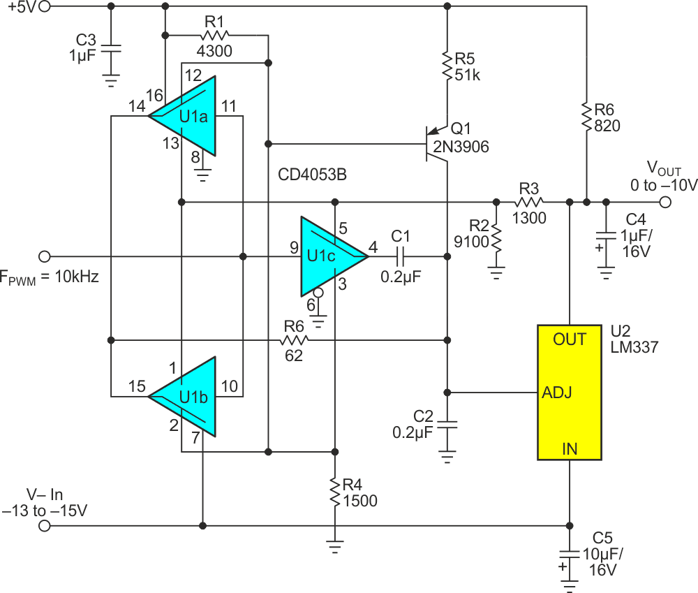
Figure 1 shows the circuit.
 |
|
| Figure 1. | LM337 joins forces with 4053 CMOS switch to make a macho PWM DAC. |
Metal gate CMOS SPDT switches U1a and U1b accept a 10-kHz PWM 5v signal to generate a +1.25 V to –8.75 V “ADJ” control signal for the U2 regulator. ADJ = +1.25 V causes U2 to output 0 V. It has always struck me somehow strange that a negative regulator like the 337 sometimes needs a positive control signal (in this case for VOUT less negative than –1.25 V), but it does. ADJ = –8.75 V makes it make –10 V.
U1c generates an inverse of the PWM signal, providing active ripple cancellation as described in “Cancel PWM DAC ripple with analog subtraction” (Reference 1).
Current source Q1 reduces zero offset error by nulling the ~65 µA (typical) ADJ pin bias current. The feedback loop established via R2 and R3 makes full-scale –10 V output proportional to U2’s internal reference as previously mentioned.
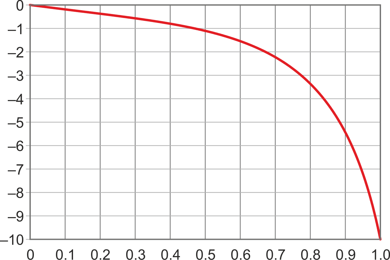
This does, however, make output voltage a nonlinear function of PWM duty factor with functionality (D from 0 to 1):

as graphed in Figure 2.
 |
|
| Figure 2. | Graph of VOUT (0 V to –10 V) versus the PWM duty factor (0 to 1). [VOUT = –1.25×D/(1 – 0.875×D)]. |
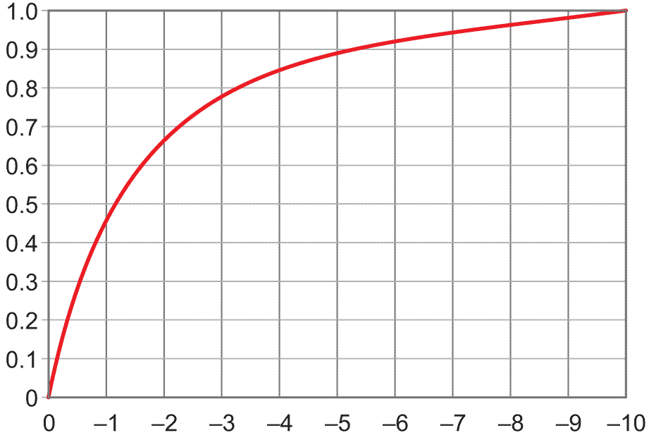
Figure 3 plots the inverse of Figure 2, yielding the PWM D required for a given VOUT.
 |
|
| Figure 3. | Graph of the PWM duty factor (0 to 1) versus VOUT (0 V to –10 V). [PWM D = VOUT/(0.875×VOUT – 1.25)]. |
For the corresponding 8-bit PWM setting

The negative supply rail (V–) can be anything between –13 V (to accommodate U2’s minimum headroom requirement) and –15 V (in recognition of U1’s maximum voltage rating). DAC accuracy will be unaffected.
U2 should be adequately heatsunk as dictated by heat dissipation equal to output current multiplied by the V– to VOUT differential. Up to double-digit Watts are possible. The 337s go into thermal shutdown at junction temperatures above 150 °C, so make sure it will pass the wet-forefinger-sizzle “spit test!”
Reference
- Woodward, Stephen. "Cancel PWM DAC ripple with analog subtraction."