Students, hobbyists, and professionals today enjoy unprecedented access to powerful and affordable test equipment for understanding and building electronic projects. But as enthusiast projects have become more advanced and ambitious, it is still possible to hit the limits of entry-level equipment. I have been excited about open source hardware as an avenue to advance the performance and accessibility of test equipment, in much the same way the early open source software focused on development tools as a foundation for greater access to computing. This article is about my experiences building an open hardware single-ended active probe.
For most of us, our experience with oscilloscope probes begins and ends with passive probes. These appear at first to be a simple resistive divider with some capacitive compensation to extend their range, but hide a number of complex tricks. For one, it’s remarkable they work at all. Transmission line theory suggests connecting a device under test (DUT), which could have any source impedance, to a long transmission line that is terminated by an unmatched load (namely, the oscilloscope front end) is recipe for signal reflections. Yet in most cases, these probes work just fine without ringing or distortion. The trick, invented by Tektronix in the 1950s (Ref..1), is to use a lossy transmission line in the probe cable by replacing the inner conductor with resistance wire. This damps signal reflections, and together with carefully chosen compensation capacitors, yields a flat, wideband response.
These methods have their limits, which mean 10× passive probes can achieve a few hundred megahertz of bandwidth and have an input capacitance of 10–20 pF. Even at lower frequencies, this capacitance is sometimes high enough to make passive probes a poor choice. A crystal oscillator uses a load capacitance that is comparable to this number, so connecting a passive probe will immediately detune the circuit.
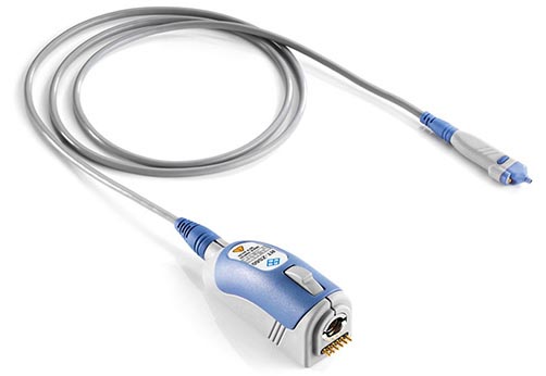
Active probes shine with high-frequency circuits or ones that require low loading, because their input capacitance is smaller by an order of magnitude (Figure 1). The operating principle behind an active probe is to use a buffer amplifier that has high input impedance and reproduces the signal at lower output impedance. The output impedance of the amplifier can be controlled to match the transmission line and oscilloscope termination for higher signal integrity. However, commercial active probes typically cost several thousand dollars. They take advantage of proprietary connectors that allow the probe to automatically configure the oscilloscope and use a single cable for power and signal, but this convenience locks you in to the vendor’s ecosystem. This usually doesn’t trouble professional labs that can afford to buy bundled packages of instruments and accessories, but it means even used active probes are often difficult for enthusiasts to work with.
 |
|
| Figure 1. | A modern commercial active probe with proprietary interface connector. |
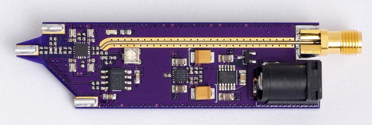
DIY designs of active probes using discrete components have been done before, but they haven’t matched the bandwidth of commercial devices, and usually lacked the flexibility of DC coupling. The recently introduced BUF802 has made it possible to overcome these limitations and build very high performing analog front ends using off-the-shelf components and low-cost designs. The BUF802 is unity-gain buffer amplifier with a bandwidth of 3 GHz. A project is now underway to build an open source oscilloscope (Ref. 2) using this chip in the front end, and I’ve been experimenting with a complementary effort to build a single-ended active probe (Figure 2), with the following design goals:
- DC–2 GHz analog bandwidth, 10:1 attenuation
- Input impedance of 1 MΩ || 1 pF, 50 Ω output impedance
- Rated performance achievable on OSH Park FR-408HR four-layer stackup (Ref. 3)
- Minimum component size of and no BGA parts
- Open source design and repairable
 |
|
| Figure 2. | PCB assembly of the prototype active probe on OSH Park’s four-layer stackup. |
Development history
The BUF802 first came to my attention in late 2022 and I began researching how to use it as an active probe amplifier. I designed a non-form-factor evaluation board where the input and output were coupled to coaxial connectors for bench testing.
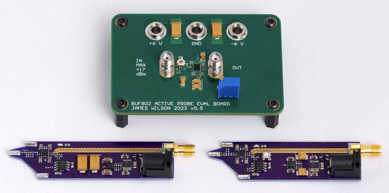
I designed and tested an initial rev A probe in late 2023 and found the location of the ground socket wasn’t optimal, and this was followed quickly by a rev B which incorporated a second ground socket without other changes (Figure 3). The rev B design was able to meet the 2 GHz bandwidth goal in testing. Since that time, I also obtained a Bode 100 VNA, which I used to examine the power distribution network and the crossover region performance. These measurements and further experiments showed the trimmable PCB capacitor used for frequency compensation was too lossy. Rev C incorporated minor optimization to PDN components and a redesign of the input network to use fixed frequency compensation capacitors, while making low-frequency attenuation trimmable. The design files and this documentation are licensed under the terms of the CERN Open Hardware License (CERN-OHL-S version 2) and are available for download in the Downloads section.
 |
|
| Figure 3. | Later evaluation board with rev B and C of the form-factor probe. |
Performance summary and methodology
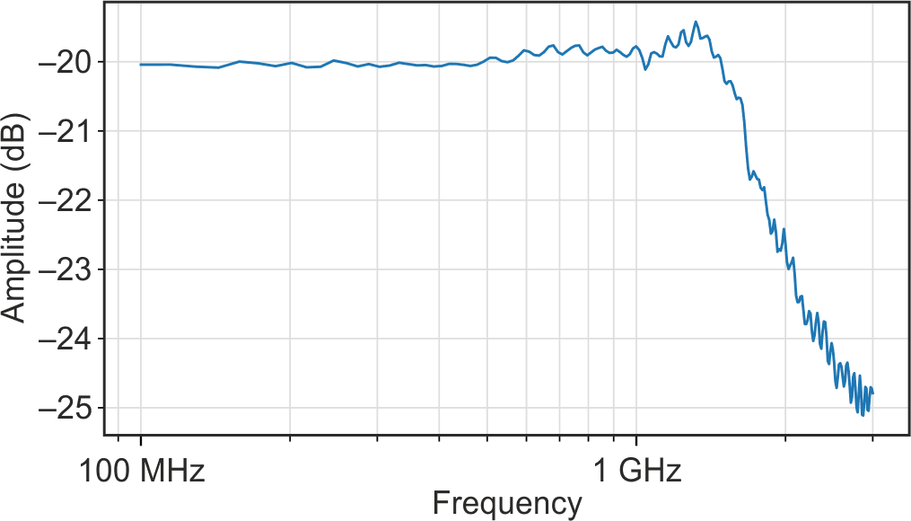
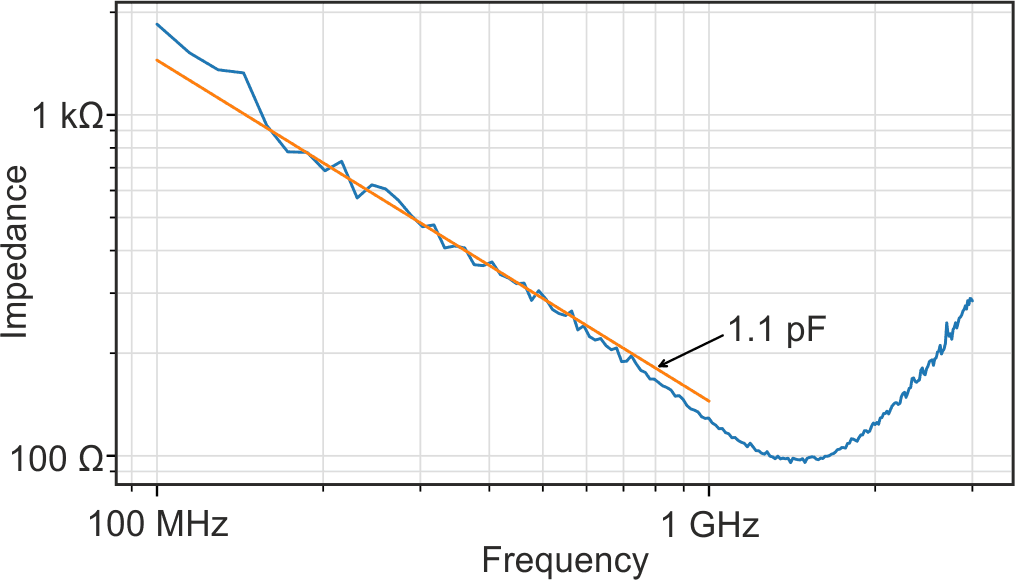
The charts in Figures 4 and 5 show the performance of the rev C probe measured on a network analyzer. The probe shows a very flat response with a 3 dB bandwidth just over 2 GHz. The input impedance is about 1.1 pF, with a ZMIN of about 100 Ω near 1.6 GHz. This is just above my original goal of 1 pF, but is hardly any disappointment.
 |
|
| Figure 4. | Probe response VOUT/VSOURCE. |
 |
|
| Figure 5. | Probe input impedance, Z. |
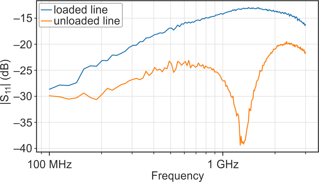
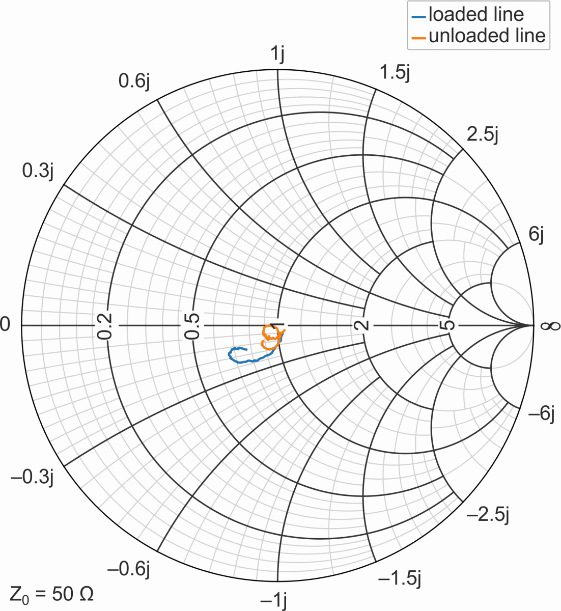
An alternative view of the input impedance is to look at return loss when the probe is used in a 50 Ω environment. Here the return loss of a 50 Ω terminated line is shown in a magnitude (Figure 6) and Smith chart (Figure 7), with and without the probe attached. The return loss of the probed line remains better than 13 dB.
 |
|
| Figure 6. | Probe input impedance, S11. |
 |
|
| Figure 7. | Probe input impedance, S11, in a Smith chart. |
There is something of an industry schism on how to properly characterize the performance of high-frequency probes. This could be called the what-was vs. what-is controversy (Ref. 4): should a probe seek to accurately reconstruct the signal that was present before the probe was attached (what was), or should it seek to show the signal as it is loaded by the impedance of the probe (what is)? In an ideal world, the probe would have infinite impedance and these two positions would converge. When the probe has finite impedance, then the voltage at the probe input VIN is no longer equal to the source/test generator output VSOURCE. Both interpretations of the probe response as VOUT/VSOURCE or VOUT/VIN are correct, but with different meanings. In the what-was camp are Tektronix and Rohde & Schwartz, while Keysight has advocated for the what-is position. Keysight argues showing the original signal masks loading problems (Ref. 2). Tektronix claims the showing the original signal is more useful, and including the probe loading effect overstates the bandwidth of the probe (Ref. 5). Both claim they’re right and a better fit for real-world probing. For my part, I tend to agree with Tektronix; I want to characterize the DUT, not the combination of the DUT and probe.
Compounding this confusion is the reality that probes are used the field where conditions vary greatly. The nature of the connections from the probe sockets to the DUT greatly impact the parasitics and performance. The probe is usually held in hand, which challenges day-to-day and person-to-person consistency. To get any hope of consistent benchmarking, vendors measure probe performance using a fixture that minimizes variation and parasitics, as have I. In one of its application notes, Keysight freely admits this means “the probe’s specified bandwidth is [typically] unachievable in any everyday, usable configuration” (Ref. 6). Consequently, bandwidth charts for any probe should be considered as a best-case scenario.
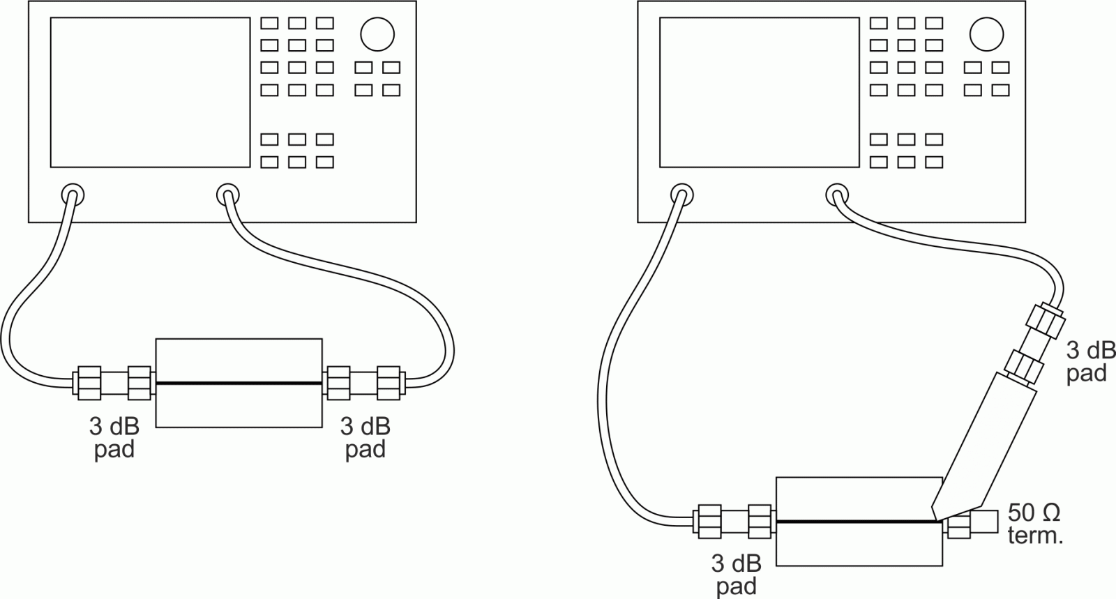
The test fixture in Figure 8 is just a PCB with a 50 Ω exposed thru line and end-launch connectors. Characterizing the probe response is done with a two-port network analyzer. First, a response calibration is made with the analyzer ports connected via the thru fixture, and then the fixture’s port 2 connection is replaced with a termination. The probe output connects to port 2, making the transfer function VOUT/VSOURCE equal to S21. The line should be probed as close to the termination as possible. To reduce ripple from minor mismatches in the measurement path and make for a cleaner chart, inline attenuators are used at the ends of the cables throughout this task.
 |
|
| Figure 8. | Two-port calibration and measurement setup for characterizing probe response. |
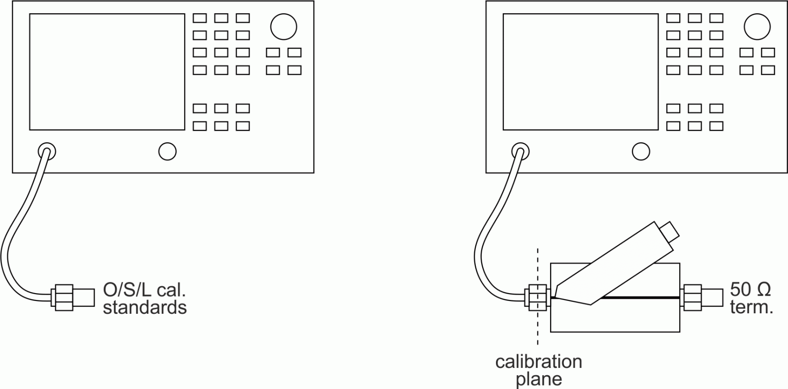
For measuring input impedance, the one-port measurement setup involves performing a calibration and then connecting the terminated thru fixture (Figure 9). The calibration plane is at the connector to the fixture, and the line must be probed as close to this point as possible. To squeeze a little more accuracy out of the calculation, I used the VNA to measure the electrical length from the calibration plane to the board/connector interface, and then added this as a port extension. This adjusts the calibration plane to almost exactly the point of contact with the probe. The return loss is measured with and without the probe connected, and then the probe input impedance can be backed out of these measurements by assuming the probe impedance is in parallel with the impedance of the terminated thru line.
 |
|
| Figure 9. | One-port calibration and measurement setup for characterizing input impedance. |
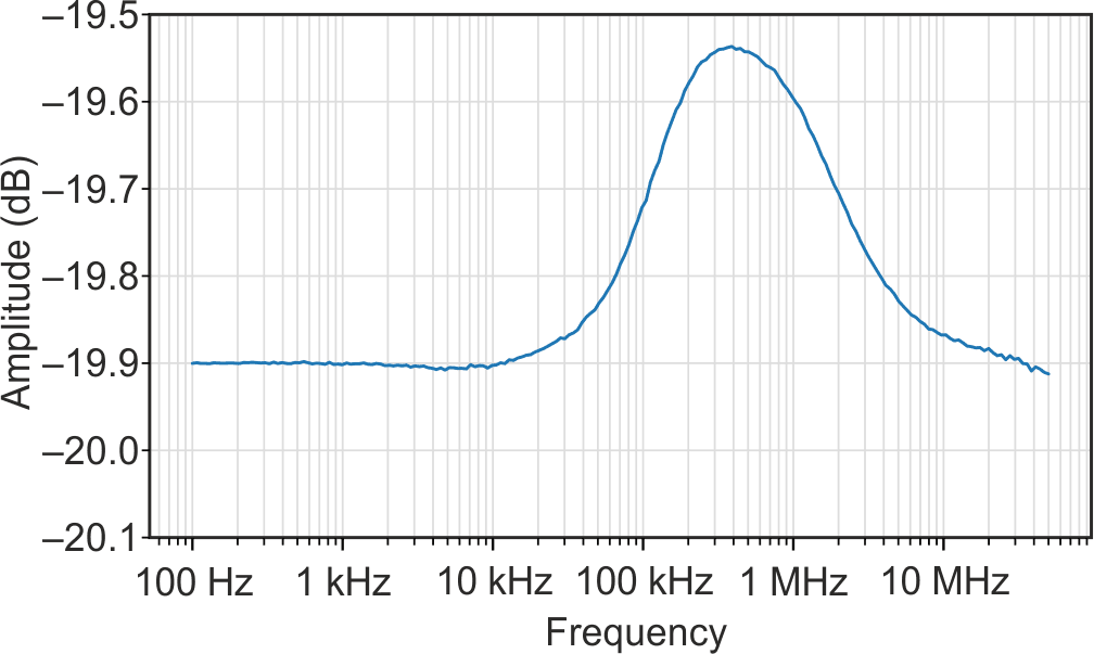
Characterization of the probe in the crossover region started with a mystery and revealed some disappointing limits on the board stackup. In the frequency range of 10 kHz to 10 MHz, the probe output transitions from being driven by feedback from the precision amplifier to following the input resistive divider, and then the capacitive divider. Ideally, the response should be flat. If the input network frequency compensation is imperfect, then one would expect to see flat regions at the low and high end, and a sloping transition between. Instead, I saw the following peaking response (Figures 10 and 11).
 |
|
| Figure 10. | Probe response VOUT/VSOURCE, crossover region. |
 |
|
| Figure 11. | Evaluation board response VOUT/VSOURCE, crossover region. |
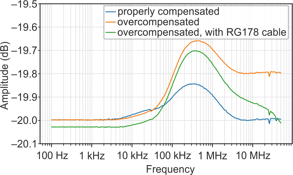
This behavior was puzzling because it didn’t appear in simulation, and also is less prominent with the evaluation board, which has only about 0.1–0.2 dB of peaking in this range when properly compensated. My first hypothesis was the combination of misadjusted frequency compensation and transmission line loss. The evaluation board provided a means to test the hypothesis: the frequency compensation capacitor is a trimmer for easy tuning, and I could interpose a length of poor cable and see if the result matched the chart. When I adjusted the frequency compensation and added a section of RG178 (a thin type of coaxial cable only suitable for short runs), the response demonstrated a similar peaking shape. Given the low frequency, the likely source of the cable loss is from conductor loss rather than dielectric loss.
References
- J. R. Kobbe and W. J. Polits. “Electrical probe,” U.S. Patent 2883619.
- ThunderScope
- 4 Layer Prototype Service
- Agilent Technologies. Side-by-Side Comparison of Agilent and Tektronix Probing Measurements on High-Speed Signals, Application Note 1491, January 2007.
- Tektronix. Probe Bandwidth Calculations, Technical Brief 60W-18324-0, November 2004.
- Keysight Technologies. Improving Usability and Performance in High-Bandwidth Active Oscilloscope Probes, Application Note 5988-8005, July 2014.
- Texas Instruments, Achieving high-DC Precision and Wide Large Signal Bandwidth with Hi-Z Buffers, Technical Article SSZT102, Jan. 2022.
Materials on the topic
- Datasheet Analog Devices ADA4625
- Datasheet Texas Instruments BUF802
- Datasheet Linear Technology LTC3261
- Datasheet Texas Instruments OPA140
- Datasheet Texas Instruments TPS7A39
- Datasheet Diodes BAT54
- Datasheet Vishay VLMTG1300