RTDs (resistance-temperature detectors) are the preferred sensor choices for designs requiring precision. Although RTDs are approximately linear over the limited temperature range of 0 to 100 °C, these sensors exhibit a slight but progressively more nonlinear temperature-versus-resistance characteristic as the measurement range widens. Consequently, over an extended span, curve fitting is necessary if the system is to achieve a high level of precision. One way to obviate the nonlinear characteristic of an RTD sensor is to design analog hardware to perform the curve-fitting mathematics before any additional signal processing occurs. This approach is especially attractive if you can keep both cost and component count low and if a microprocessor-driven design is not feasible. With low component count comes the added benefit of a small PCB (printed-circuit-board) footprint.
 |
|
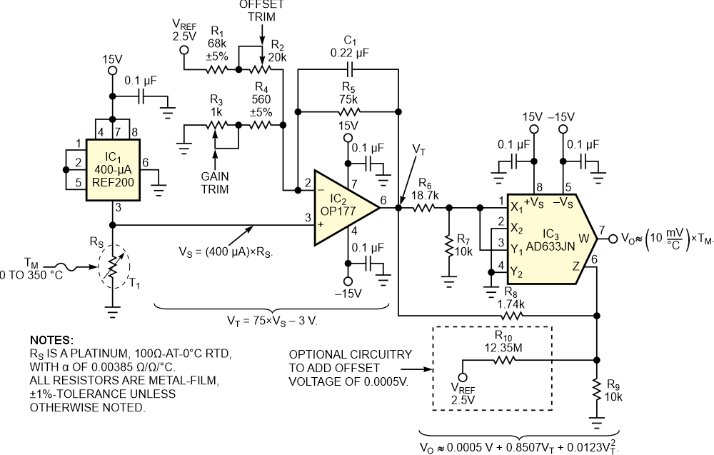
| Figure 1. | This RTD circuit uses a second-order polynomial to linearize the output of the sensor. |
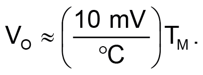
The most popular RTDs are made from platinum with a resistance value of 100 Ω at 0 °C and a metal purity that allows them to follow a standard European curve with a positive-temperature coefficient, α, equal to 0.00385 Ω/Ω/°C. Less popular but still common are RTDs with a slightly higher metal purity. These RTDs have α of 0.00392 Ω/Ω/°C and follow the US curve. The circuit in Figure 1 uses a standard RTD to measure temperature over the extended range of 0 to 350 °C, an output voltage of 0 to 3.5 V, and overall system accuracy greater than 0.5 °C. The following linear equation expresses this sensor system:
IC1 is pin-configured to drive a constant current of 400 µA through the grounded sensor, T1. Driving T1 with this level of current – “zero-power” operation – keeps the worst-case power that the circuit dissipates in the sensor to less than 40 µW and reduces the self-heating errors to a second-order effect (Reference 1). Also, driving the RTD with a current source preserves its intrinsic nonlinearity and allows you to express the sensor’s output voltage, VS, as: 400 µA × RS, where RS is the resistance of the sensor.
IC2 initially signal-conditions the sensor’s output by first scaling the output voltage and then offsetting the result so that VT is slightly larger than the 3.5 V output at 350 °C and that VT equals 0 V at 0 °C. Adding gain and offset before linearization places less of a burden on the curve-fitting circuitry and helps to meet the system’s precision specification. The combination of C1 and R5 implements a lowpass filter with a pole at approximately 10 Hz to remove power-supply noise. The following term describes the performance of IC2 and its accompanying circuitry: VT = 75VS – 3 V.
Next, an Excel spreadsheet creates the nonlinear-mathematical relationship between the voltage, VT, and the system output, VO (Table 1). The spreadsheet features 17 temperature entries – starting at 0 °C, increasing in increments of 25 °C, and ending at 400 °C – for the measured temperature. Using a data set that extends beyond the intended measurement range of 350 °C can reduce end errors in nonlinear systems. Values for RS – which you derive from a standard RTD-resistance-versus-temperature table – and the equations allow you to compute VS and VT. The VT and VO columns are the input and output signals, respectively, for the linearization circuitry; you chart them using Excel’s XY-scatter feature. You can use Excel’s Trendline feature to create the following equation, the mathematical representation of the curve-fitting circuitry you need to linearize the sensor’s output:

| Table 1. | Excel-spreadsheet data | ||||||||||||||||||||||||||||||||||||||||||||||||||||||||||||||||||||||||||||||||||||||||||
|
|||||||||||||||||||||||||||||||||||||||||||||||||||||||||||||||||||||||||||||||||||||||||||
IC3 and four 1%-tolerant resistors or, optionally, five resistors implement a second-order polynomial:
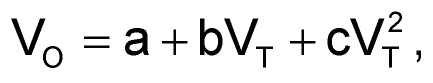
where a is the offset term, b is the linear coefficient, and c is the square-term coefficient.
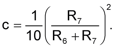
The curve-fitting-circuit design begins by first wiring the four inputs of IC3 to create a positive square term that is scaled at the chip’s output by an internal scale factor of 1/10 V. Then, comparing terms, you find that the coefficient, c, must equal 0.0123. Because R6 and R7 form a voltage divider that attenuates the signal, VT, you can express the coefficient with the following equation:
Select a value for R7 – 10 kΩ for this design – and then use the preceding equation to find the value for R6.
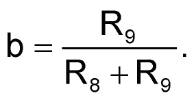
Resistors R8, R9, and, optionally, R10 form a passive adder to create the offset term, a, and the linear coefficient, b. You apply the output of the passive adder directly to the Z input, Pin 6 of IC3, which adds the offset and linear terms to the square term to form the system response at Pin 7. Again comparing these terms, note that the offset term must equal 0.0005 V. The offset term is only 0.5 mV, and eliminating it would add an error of approximately 0.05 °C, so you can initially neglect it. Then, because the linear term’s coefficient, b, must equal 0.8507, you first select a suitable value for R9 and use the following equation to solve for R8:
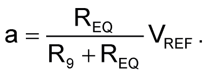
If you wish to design the optional circuitry and include the offset term, which is part of the passive adder, choose a stable 2.5 V reference for VREF, calculate the parallel combination of R8 || R9 = REQ (the equivalent resistance of R8 in parallel with R9), and solve for R10 using the following voltage-divider equation:
To calibrate this circuit, replace the sensor with a precision decade box. Set the decade box to simulate 0 °C and adjust the offset trim of R2 for an output of 0 V at Pin 7 of IC3. Next, set the decade box to simulate 350 °C and adjust the gain trim of R3 for an output of 3.5 V. Repeat this sequence of trim steps until both points are fixed. The circuit in Figure 1 – which includes optional circuitry – exhibits a worst-case measurement error at 250 °C and 2.504 V of 0.16%, or 0.4 °C. Testing the circuit without the optional circuitry – the reference voltage and R10 – shows no discernible improvement in precision.