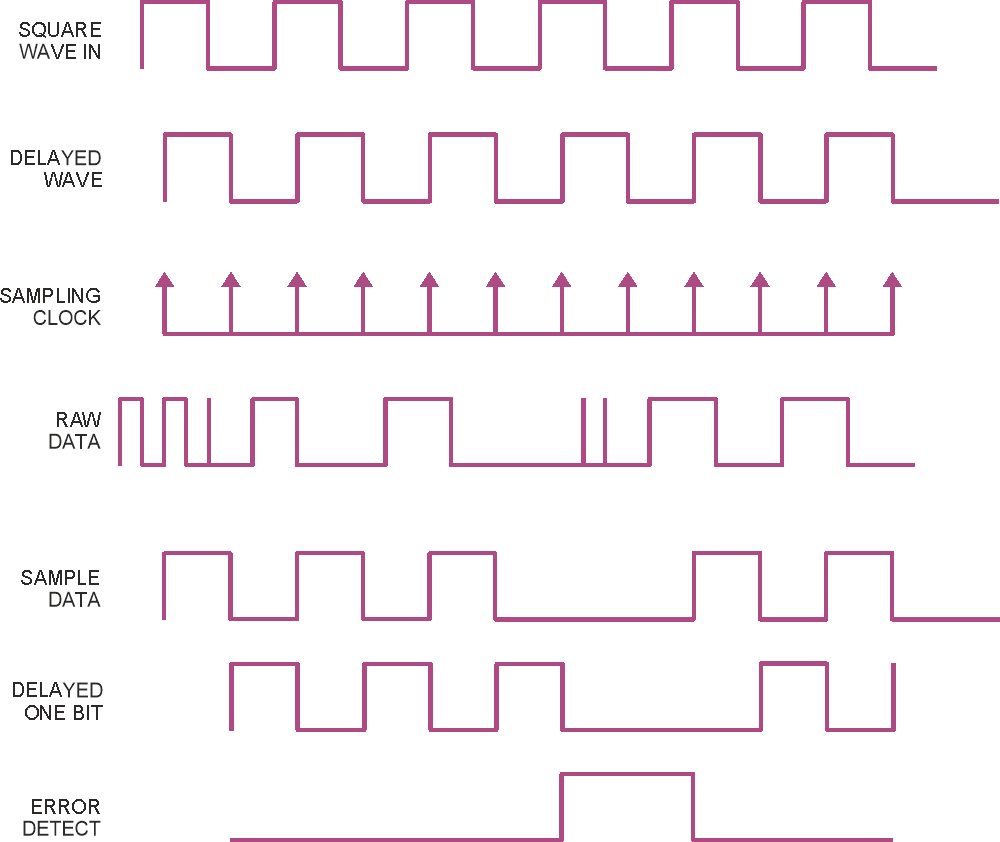
Traditionally, the reception quality of a digital receiver is expressed in terms of BER (bit-error rate). This figure is the proportion of received bit errors in a given period. Typically, you measure the BER in the lab by applying an RF signal, modulated by a pseudorandom code, to the receiver under test. This Design Idea suggests an alternative method based on the use of a simple square wave. This method may not be superior to the usual technique, but it is simple to implement and gives a reliable result. The simplicity of the method is based on the fact that it requires no complex synchronization. Admittedly, a square wave is not truly representative of the data a receiver encounters in normal use (Figure 1). The square wave to modulate the RF carrier is phase-shifted to allow for the delay in the receiver. An exclusive-OR gate produces a sampling pulse at each bit transition – typically, 10% of the data-bit width. This sample pulse samples the raw data the receiver generates, producing clean data.
 |
|
| Figure 1. | This timing diagram illustrates the operating principles of a simple BER tester. |
The key to understanding this technique is to keep in mind that a string of two successive ones or zeros indicates an error. A D flip-flop implementing a 1-bit delay detects the error.
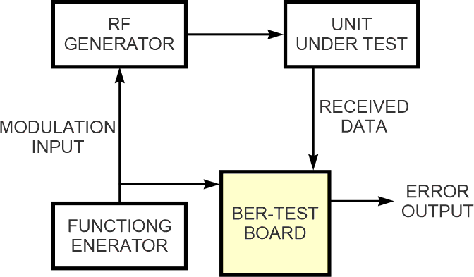
You can display error pulses on an oscilloscope or count them by using a frequency counter. Figure 2 shows a typical test setup. You modulate the RF generator at the prescribed data rate. Note that a 500-Hz square wave is equivalent to a baud rate of 1 kbps. Both the modulating signal and the received data feed into the BER-test board. You adjust the sampling signal to be near the end of the received-data pulse. In many digital receivers, this arrangement yields a fair approximation to a correlation receiver. Error pulses appear on the oscilloscope. If you wish, for example, to set the RF level for a BER of 1-to-100, you reduce the RF level to the receiver such that, in a 100-msec sweep you see, on average, one error pulse per sweep.
 |
|
| Figure 2. | The BER tester uses a signal generator with OOK (on/off-key) modulation |
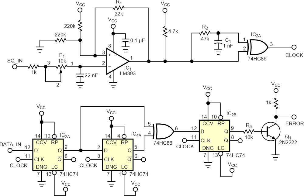
In Figure 3, IC1 and potentiometer P1 form the basis of an adjustable phase shifter. R2 provides hysteresis, and R1, C1, and IC2 form a differentiator that provides a sampling pulse train. The first flip-flop clocked by the sampling pulse makes a hard decision concerning each bit. The next D flip-flop, together with exclusive-OR gate IC2B detects the occurrence of two successive identical bits. This situation constitutes an error. A final D flip-flop and a transistor ensure that the Error output is clean.
 |
|
| Figure 3. | The simple BER tester uses an adjustable phase shifter and a differentiator. |
The construction of the system follows the circuit diagram in Figure 3. It sets an HP8647 RF signal generator at 868.35 MHz, and a function generator provides OOK (on/off-key) modulation. The receiver under test was a Melexis TH7122 at 868.35 MHz in the OOK-modulation mode. Adjust the RF level to vary the error rate. This design obtains an RF level of –107 dBm for a 1-to-1000 BER and –108 dBm for a BER of 1-to-100, levels consistent with the data sheet. You should take care when you're implementing OOK. Most RF generators provide AM. Thus, you must remove 3 dB from the displayed RF value. You can use this technique for other types of binary modulation, such as FSK (frequency-shift keying), for example.