This modular resistor load bank uses a unique topology to reduce the number of switches and resistors while providing the maximum number of steps.
An array or bank of load resistors is often required for testing power products, characterization of solar panels, and many other applications that require evaluation under various well-defined loads. While simple rheostats can provide continuous variation in load resistance, their power rating decreases as the value of their resistance is decreased, and they have series inductance that’s undesirable in some cases. Instead, a resistor “load bank” is a better alternative.
Some of the features that engineers look for with a load-resistor bank are:
- The series inductance should be as low as possible.
- The number of steps should be as large as possible.
- As the load resistance is reduced, the power rating should go up.
- It should have a low component count.
This modular resistor load bank topology, which uses four switches and five resistors, also acts as a building block (Fig. 1). It varies the resistance value in 12 steps; if more than 12 steps are required, another such module can be connected in parallel, thus increasing the number of steps to 144. In this way, it’s possible to get a large number of steps without increasing the complexity.
 |
|
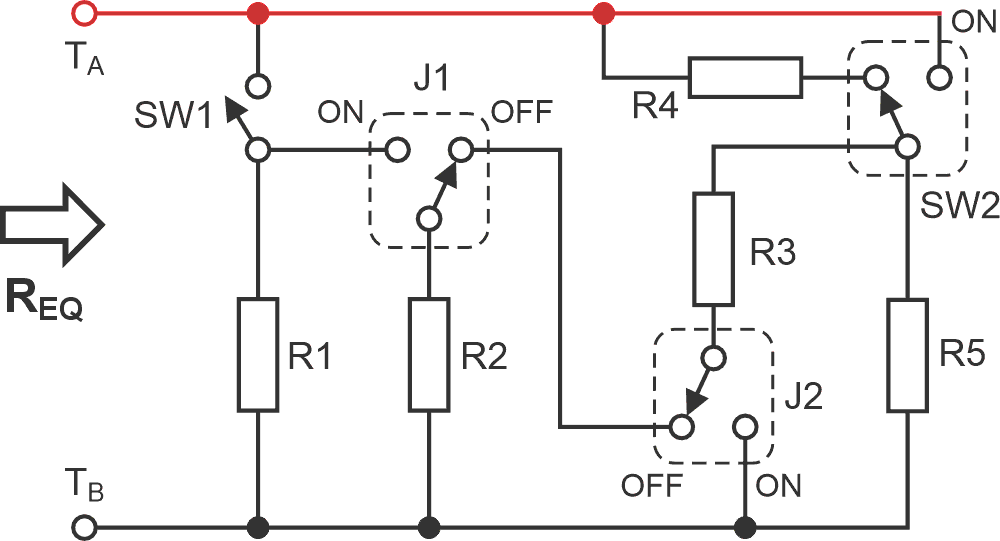
| Figure 1. | The load-resistor bank topology with four switches and five resistors is straightforward. |
The basic resistor load bank consists of resistors R1 through R5 and switches SW1, J1, J2 and SW2. Switch SW1 is used to control R1 and R2, while switch SW2 is used to control R4 and R5. One end of R2 and R5 is directly connected to ground, while R2 and R3 are connected through jumper switches J1 and J2 to ground. Table 1 shows the equivalent resistance REQ for the various combinations of switch settings.
| Table 1. | Resistor combinations for different switch settings and corresponding equations | |||||||||||||||||||||||||||||||||||||||||||||||||||||||||||||||||||||||||||||||||||||||||||||||||||||||||||||||||||||
|
||||||||||||||||||||||||||||||||||||||||||||||||||||||||||||||||||||||||||||||||||||||||||||||||||||||||||||||||||||||
With four switches, 16 switch-setting combinations are possible. There are 12 distinct values for REQ, using 12 switch settings. (The remaining four switch settings produce repeat values for REQ; these alternate settings are captured in the column labeled “Alt.”) Equations for calculating the value of REQ for 12 distinct combinations are given in the column “Equations,” while the column “Alt Equations” lists equations for alternate combinations.
The division/multiplication factors for 12 switch settings needed to calculate REQ are in the column “Factor.” These factors have been derived when all five resistors are of same value equal to R Ω. The values shown in column “REQ” have been calculated for the case R1 = R2 = R3 = R4 = R5 = 1000 Ω.
With all resistors at 1000 Ω /2 W, the resulting specifications are:
- REQ (maximum) = 2000 Ω.
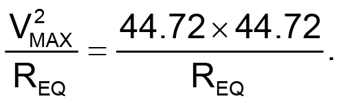
- Maximum voltage that can be applied = VMAX = √(2 × 1000) = 44.72 V.
- Power rating at REQ (maximum) resistance = 1 W
- REQ (minimum) = 250 Ω.
- Power rating at REQ (minimum) resistance = 8 W.
- Power rating at any other resistance setting:
 |
|
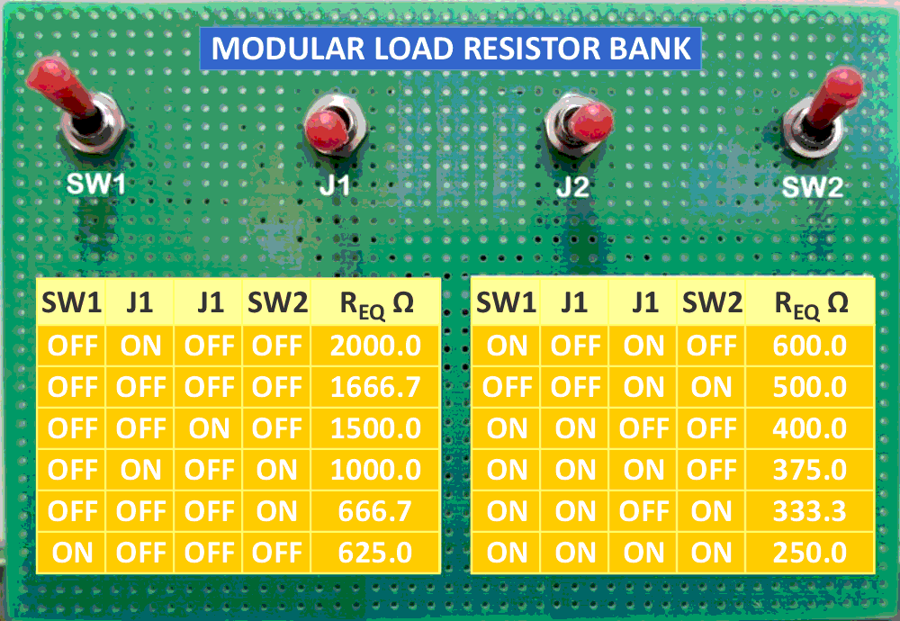
| Figure 2. | This view of the front panel shows 12 unique resistance values for R = 1000 Ω. |
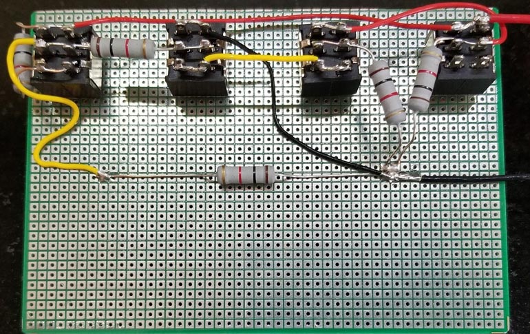
Figure 2 shows the front panel of the load bank, while Figure 3 shows the mounting arrangement of switches and resistors.
 |
|
| Figure 3. | Mounting of switches and resistors on the printed wiring board is non-critical. |
This simple resistor load bank is very compact and cost-effective. It uses very few components and can produce 12 different load-resistor values. However, some situations require a larger number of steps.
Using multiple load banks for a larger number of steps
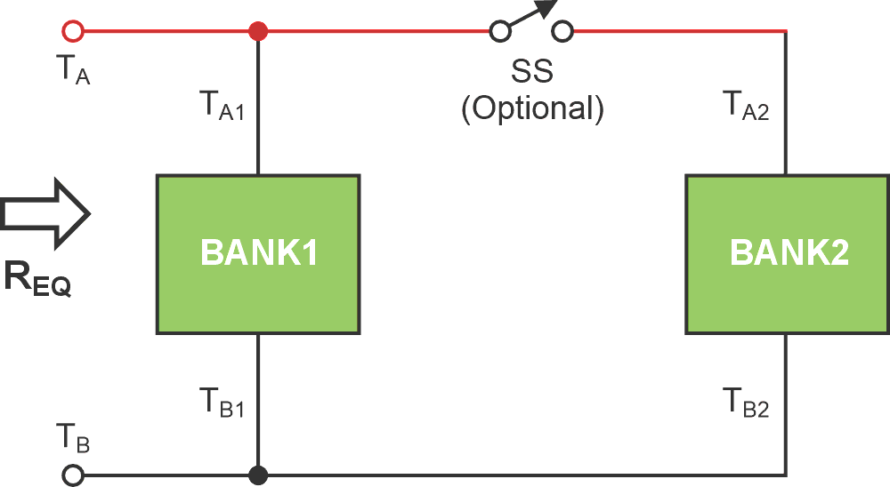
Using the basic load bank module described above, with two modules simply connected in parallel, enables the generation of more steps (Fig. 4). For each setting of resistance for BANK1, we have 12 different settings of BANK2.
The equivalent resistance of load bank is given by:
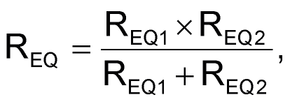
where REQ1 is the equivalent resistance of BANK1 and REQ2 is the equivalent resistance of BANK2.
There are two ways in which the load banks can be interconnected:
Interconnection with a switch in series
As shown in Figure 4, two load banks are connected through a switch SS. When SS is ON, both banks are connected in parallel. When SS is in the OFF position, only BANK1 is active. Total number of steps generated in this case is determined as follows:
- When SS is OFF, the number of steps generated using BANK1 = 12.
- When SS is ON, the number of steps generated using BANK1 and BANK2 = 12 × 12 = 144.
 |
|
| Figure 4. | The parallel connection of two load banks enables an increased number of steps for REQ. |
Therefore, the total number of steps = 12 + 144 = 156. Thus, by adding one extra switch, we get the benefit of 12 extra steps.
Interconnection without switch in series
In this case, switch SS isn’t present and both banks are permanently connected. Hence, total number of steps is 144.
Selection of resistor values
The selection of resistor values is important. If the two load-resistor banks have identical resistor values, then a large number of duplicate values will be generated. Therefore, it makes sense for the two banks to use slightly different values. Consider the case where all five resistors of BANK1 are 1000 Ω while those of BANK2 are 910 Ω. The equivalent resistor values for both the banks are shown in Table 2.
| Table 2. | REQ values for BANK1 and BANK2 for 12 switch setting. | |||||||||||||||||||||||||||||||||||||||
|
||||||||||||||||||||||||||||||||||||||||
Using these two load banks, Table 3 shows the generated resistor values.
| Table 3. | REQ values in ohms for the load bank of Figure 4 | |||||||||||||||||||||||||||||||||||||||||||||||||||||||||||||||||||||||||||||||||||||||||||||||||||||||||||||||||||||||||||||||||||||||||||||||||||||||||||||||||||||||||||||||||||||||||||||||||||||
|
||||||||||||||||||||||||||||||||||||||||||||||||||||||||||||||||||||||||||||||||||||||||||||||||||||||||||||||||||||||||||||||||||||||||||||||||||||||||||||||||||||||||||||||||||||||||||||||||||||||
For this table, note that:
- If switch SS isn’t used, then values in column “SS OFF” will not be available.
- All resistor values have been rounded off to 1 Ω.
- Choose adjacent values for BANK1 and BANK2; if the resistor values are spaced wide apart, then the power rating of the resistors is reduced.
For two banks connected in parallel, with all resistors of BANK1 at 1000 Ω/2 W and all those of BANK2 at 910 Ω/2 W, the resulting load-bank specifications are:
- REQ (maximum) = 2000 Ω when switch SS is included
- REQ (maximum) = 953 Ω when switch SS isn’t included
- Maximum voltage that can be applied = VMAX = √(2 × 910) = 42.66 V
- Power rating at REQ (maximum) = 0.9 W (with SS)
- Power rating at REQ (maximum) = 1.9 W (without SS)
- REQ (minimum) = 119 Ω
- Power rating at REQ (minimum) = 15.3 W
- Power rating at any other resistance setting = (42.66 × 42.66)/REQ
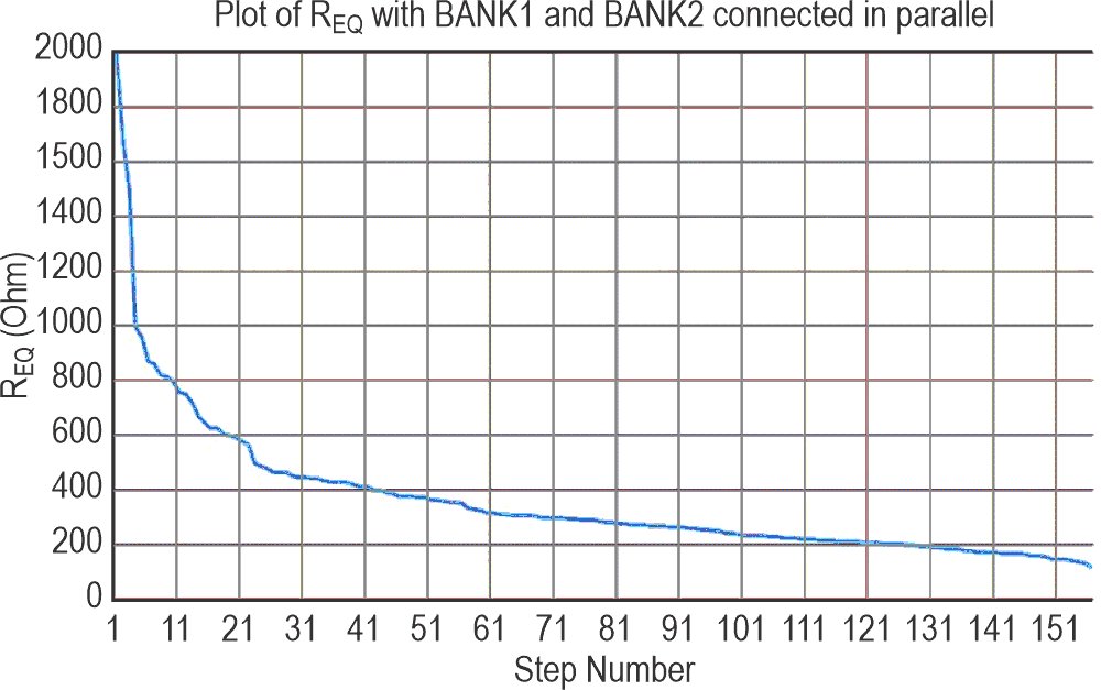
Resistance plot
Figure 5 shows a plot of load bank resistance REQ against the step number (with SS). The step number has been sequenced for getting monotonically decreasing resistance values. If switch SS isn’t used, the 12 values shown in the column “SS OFF” will not be plotted, and there will be only 144 steps.
 |
|
| Figure 5. | The variation in REQ with BANK1 (R = 1000 Ω) and BANK2 (R = 910 Ω) resistors (with SS), with the step number sequenced for obtaining monotonically decreasing resistance values. |
How to Increase number of steps in the basic topology
As shown in Figure 1, the use of four switches results in 16 switch combinations. However, Table 1 shows four alternate switch combinations that produce duplicate values of resistances. This reduces number of steps to 12. By increasing the number of steps in this basic topology itself, the overall step numbers will increase – without an increase in component count. Consider an alternate combination of 1001 in Table 1: R3 is present only in the alternate equation. Similarly, for an alternate combination of 1011, R3 is only present in an alternate equation.
Therefore, if we use different resistor values for R2 and R3, it’s possible to get two additional steps.
For BANK1: For R1 = R2 = R4 = R5 = 1000 Ω, and R3 = 953 Ω, for the first combination of 1100 → 400 Ω and for the alternate combination of 1001 → 398.1 Ω. The situation is similar for the first combination of 1101 → 333.3 Ω and for the alternate combination of 1011 → 327.9 Ω.
For BANK2: For R1 = R2 = R4 = R5 = 910 Ω, and R3 = 1100 Ω, for the first combination of 1100 → 364 Ω and for the alternate combination of 1001 → 371 Ω; for the first combination of 1101 → 303.3 Ω and for the alternate combination of 1011 → 321.9 Ω.
Therefore, the load banks can produce 14 steps each. Using the above values for BANK1 and BANK2 yields 196 steps without SS and 210 steps with SS. Thus, without any additional cost, there’s further improvement in the number of steps for REQ.
The basic load-resistor bank topology is less complex and uses fewer components. However, if a greater number of steps is required, two banks can be connected in parallel as the load bank design is modular. Using simple algorithms, it’s possible to program the load bank to generate resistance values in an increasing or decreasing stepped fashion. Due to its simplicity and modular approach, this load-bank topology should find widespread use and may even find application as a resistance “synthesizer” inside an IC.
Reference:
- Instructables (Autodesk), Vijay Vasant Deshpande, “Switched Load Resistor Bank With Smaller Step Size.”
