There’s been a lot of interesting conversation and DI teamwork lately devising circuits for ON/OFF power control using inexpensive momentary-contact switches (See Ref. 1 – Ref. 4).
Most of these designs have incorporated edge triggered flip/flops (e.g. the CD4013) but of course other possibilities exist. Figure 1 shows one of them.
 |
|
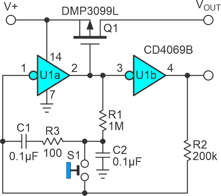
| Figure 1. | Flip/flop-free debounced push ON push OFF toggling with power-on reset and low parts count. |
Okay, I can (almost) hear your objection. It isn’t (technically) accurate to describe Figure 1 as flip/flop free because the two inverters, U1a and U1b, are connected as a bistable latch. That is to say, a flip/flop. It’s really how its state gets toggled by S1 that’s different. Here’s how that works.
While sitting in either ON or OFF with S1 un-pushed, U1a, being an inverter, charges C2 to the opposite state through R1. So, when S1 gets mashed, C2 yanks U1a’s input, thereby toggling the latch. The R1C2 time-constant of 100 ms is long enough to guarantee that if S1 bounces on make, as it most assuredly will, C2’s complementary charge will ride out the turbulence.
Then, because R2 < R1, the positive feedback through R2 will overpower R1 and keep the same polarity charge on C2 for as long as S1 is held closed. This ensures that later, when S1 is released, if it bounces on break (as some switches are rumored to be evil enough to do), the new latch state won’t be lost. PFET Q1 now transfers power to the load (or doesn’t). Thus, can we confidently expect reliable flipping and flopping and ONing and OFFing.
So, what’s the purpose of C1? Figure 2 explains.
 |
|
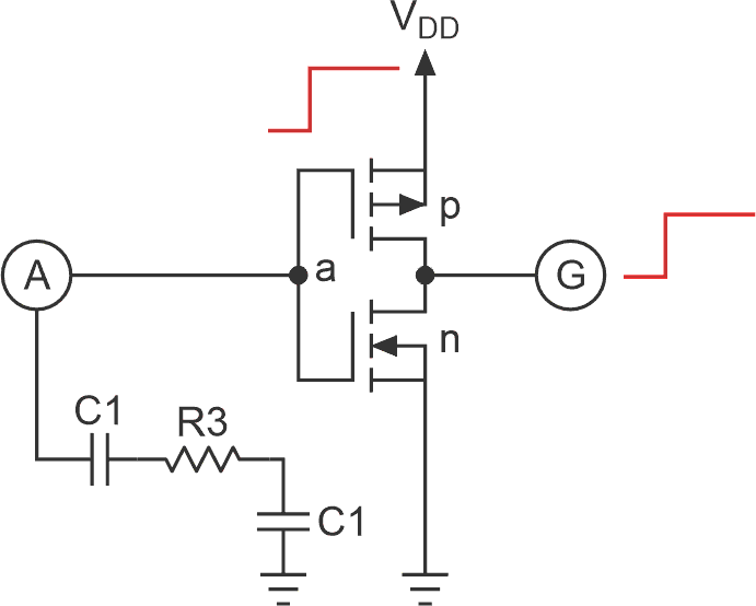
| Figure 2. | Power up turn off where the rising edge of V+ at PFET a’s source with its gate held low by RCs turns it on. |
If V+ has been at zero for awhile (because the battery was taken out or the wall wart unplugged), C1 and C2 will have discharged likewise to zero (or thereabouts). So, when V+ is restored, they will hold the inverter’s FET gates at ground. This will make the PFET’s gate negative relative to its (rising) source, turning it on, pulling its output high, and resetting the latch to OFF.
So why R3?
When the latch sits for a while with S1 unpushed, whether ON or OFF, C1 will charge to V+. Then, when S1 is depressed (note this doesn’t necessarily mean it’s unhappy), C1 will be “quickly” discharged. Without R3, “quickly” might be too much of a good thing and involve a high enough instantaneous current through S1, and hence enough energy deposited on its contacts, to shorten its service life.
Here’s a final thought about parts count. The 4069 is a hextuple part, this makes Figure 1’s use of only two of its six inverters look wasteful. We can hope the designer can find a place for the unused elements elsewhere in their application, but what if she can’t?
Then it might turn out that Figure 3 will work.
 |
|
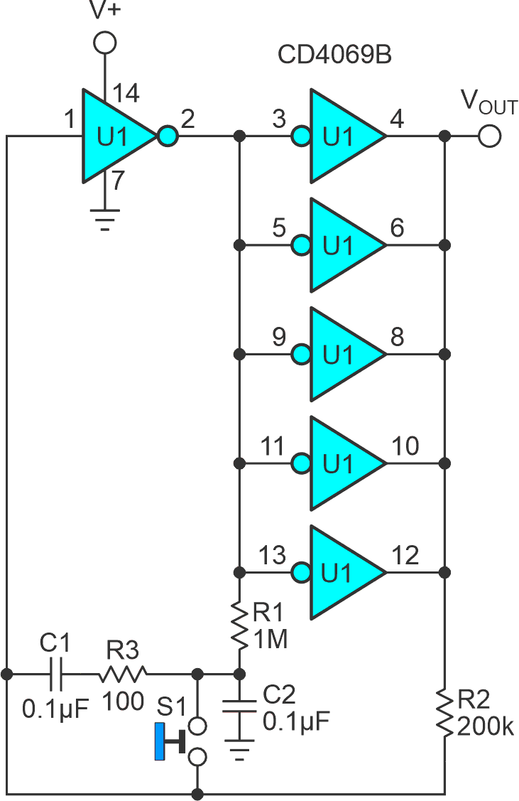
| Figure 3. | Do something useful with the other 2/3rds of U1, eliminate Q1 for loads of less than 10 mA, and gain short-circuit protection for free. |
RON for the 4069 is V+ dependent but can range as low as 200 Ω (typical) at V+ > 10 V. Therefore, if we connect all five of the available inverters in parallel as shown in Figure 3, we’d get a net RON of 200/5 = 40 Ω from V+ to VOUT. This might be adequate for a low power application, making Q1 redundant. As an added benefit, an accidental short to ground will promptly and automatically turn the latch and the shorted load OFF. U1 will therefore be that much less likely to catch fire, and us to be unhappy! Note it also works if the latch is OFF and the output gets shorted to V+.
References
- Cornford, Nick. "To press on or hold off? This does both."
- Woodward, Stephen. "Flip ON flop OFF."
- Nother, Chris. "Latching D-type CMOS power switch: A “Flip ON Flop OFF” alternative."
R Jayapal. "To press ON or hold OFF? This does both for AC voltages."
