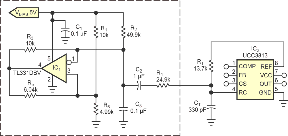
Switching power supplies can be notorious noise generators. You should prevent this noise, which is conducted, radiated, or both, from returning to the input source, where it can potentially wreak havoc on other devices operating from the same input power. The goal of an EMI (electromagnetic-interference) filter is to block this noise and provide a low-impedance path back to the noise source. The larger the noise, the greater the size, expense, and difficulty of the filter design. Power supplies that operate at a fixed frequency have their largest EMI emission at this fundamental, fixed frequency. Emissions also occur at multiples of the switching frequency but at diminished amplitudes. The simple circuit in Figure 1 makes the switching converter operate over multiple frequencies rather than one, thereby reducing the time average at any one frequency. This scheme effectively lowers the peak emissions.
 |
|
| Figure 1. | A low-frequency oscillator ramp, injected into the RC pin, modulates the supply’s switching frequency. |
The circuit in Figure 1 is a self-starting oscillator with an oscillation frequency of approximately 500 Hz. When you apply power, C3 begins to charge up from 0 V, and the output of the TL331 comparator is in a high-impedance state because its noninverting input sees a higher voltage than that of the inverting input. As C3 charges, its voltage crosses the voltage reference of the R1-R6 divider, and the comparator output trips to a low state. The voltage on R6 instantly drops to a lower reference level because R5 is now in parallel with R6. C3 begins to discharge toward this new reference level because R3 is simultaneously in parallel with C3. The cycle repeats after C3 discharges to the voltage on R6 when the comparator output reopens. You must carefully select the components to ensure that the two voltage-reference states of R6 are lower than the upper and lower possible charge states of C3. The circuit uses C3 to adjust the oscillator frequency; you should select C3 to have a lower value than C2. The oscillator’s frequency is approximately equal to
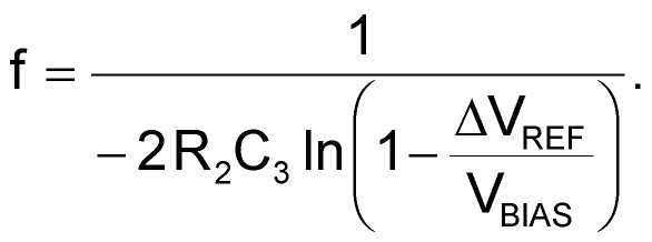
Capacitor C2 ac-couples the ramp voltage of C3 into the UCC3813’s oscillator pin. The injected signal adds to the charging current of CT during its positive portion (ac signal), thus increasing the controller’s operating frequency. During the injected signal’s negative portion, some of CT’s charging current disappears, slowing the controller’s operating frequency. Figure 2 shows the effects of the injected signal on the charging of CT. R4 controls the magnitude of the current that is injected. Reducing R4’s value increases the range, or spread, of the operating frequency around its nominal fixed frequency. The injected signal’s oscillation frequency, which C3 sets, controls the frequency-sweep rate.
 |
|
| Figure 2. | The external oscillator varies the charging of the timing capacitor. |
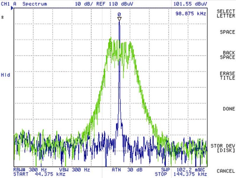
The differential EMI-current measurement of Figure 3 (1 dBµV = 1 dBµA) shows the before-and-after effects of adding the frequency-shifting oscillator. This design easily achieves a 10-dBµA reduction with a 12-kHz sweep window. A wider window further reduces EMI, but the modulator frequency may be noticeable in the converter’s output ripple voltage. It is also desirable to make the injected ramp voltage as linear in shape as possible to prevent the switching converter from spending excess time at its switching-frequency limits. The nonlinearity can result in an EMI response with two distinct frequencies. You must take care not to operate the circuit below the power converter’s low-frequency limits, or saturation of magnetics may occur. This circuit demonstrates a low-cost, small-area approach to reducing conducted-EMI emissions.
 |
|
| Figure 3. | The EMI of the flyback converter differs with and without external modulation. |
