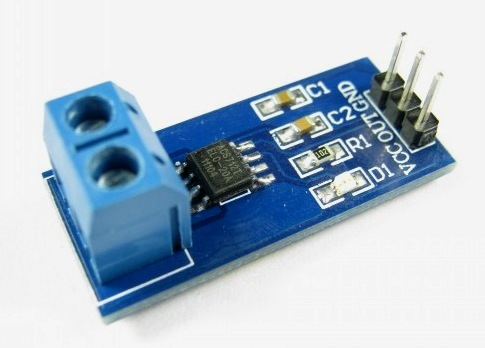
Sensing and controlling current flow is a fundamental requirement in a wide variety of applications including, over-current protection circuits, battery chargers, switching mode power supplies, digital watt meters, programmable current sources, etc. One of the simplest techniques of sensing current is to place a small value resistance (also known as Shunt resistor) in between the load and the ground and measure the voltage drop across it, which in fact, is proportional to the current flowing through it. Whereas this technique is easy and straightforward to implement, it may not be very precise because the value of the shunt resistor slightly varies with its temperature, which in fact is not constant because of the Joule heating. Besides, this simple technique does not provide an isolation between the load and current sensing unit, which is desirable in applications involving high voltage loads. Today, we will talk about Allegro ACS712 device which provides an economical and precise way of sensing AC and DC currents based on Hall-effect. This discussion is divided into two parts. The first part will provide a brief overview of the ACS712 sensor and its characteristics. In the second part, a test experiment will be carried out to interface the sensor with a PIC microcontroller to measure a dc current.
|
|
|
| Allegro ACS712. |
Theory
The current sensing technique based on a shunt resistor is described in How to measure dc current with a microcontroller? and implemented in the Multi-functional power supply project. The major disadvantages of this technique are:
- load is lifted from the direct ground connection
- non-linearity in the response due to Joule heating that drifts the resistance value
- lack of electrical isolation between the load and the sensing part
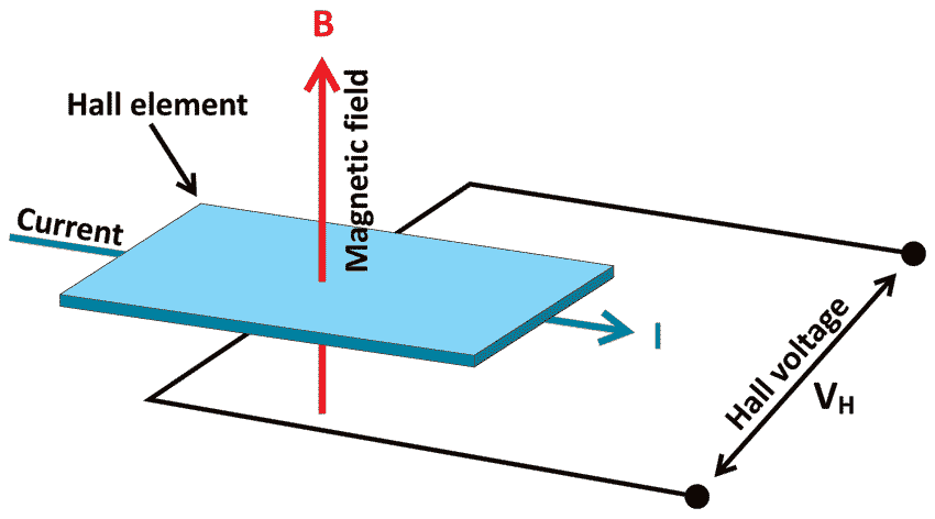
The Allergo ACS712 current sensor is based on the principle of Hall-effect, which was discovered by Dr. Edwin Hall in 1879. According to this principle, when a current carrying conductor is placed into a magnetic filed, a voltage is generated across its edges perpendicular to the directions of both the current and the magnetic field. It is illustrated in the figure shown below. A thin sheet of semiconductor material (called Hall element) is carrying a current (I) and is placed into a magnetic field (B) which is perpendicular to the direction of current flow. Due to the presence of Lorentz force, the distribution of current is no more uniform across the Hall element and therefore a potential difference is created across its edges perpendicular to the directions of both the current and the field. This voltage is known Hall voltage and its typical value is in the order of few microvolts. The Hall voltage is directly proportional to the magnitudes of I and B. So if one of them (I and B) is known, then the observed Hall voltage can be used to estimate the other.
|
|
|
| Principle of Hall-effect. |
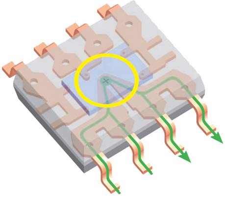
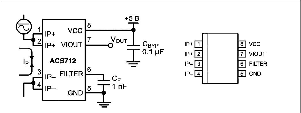
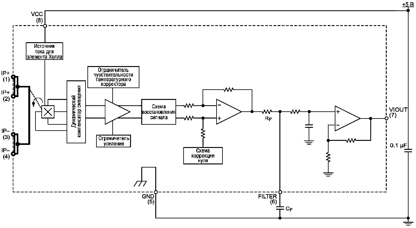
The ACS712 device is provided in a small, surface mount SOIC8 package. It consists of a precise, low-offset, linear Hall sensor circuit with a copper conduction path located near the surface of the die. When current is applied through the copper conductor, a magnetic field is generated which is sensed by the built-in Hall element. The strength of the magnetic field is proportional to the magnitude of the current through the conduction path, providing a linear relationship between the output Hall voltage and input conduction current. The on-chip signal conditioner and filter circuit stabilizes and enhances the induced Hall voltage to an appropriate level so that it could be measured through an ADC channel of a microcontroller. The pin diagram of ACS712 device and its typical application circuit is shown below. Pins 1, 2 and 3, 4 forms the copper conduction path which is used for current sensing. The internal resistance of this path is around 1.2 mΩ, thus providing low power loss. As the terminals of this conduction path are electrically isolated from the sensor leads (pins 5 through 8), the ACS712 device eliminates the risk of damaging the current monitoring circuit due to the high voltage on the conduction side. The electrical isolation between the conduction current and the sensor circuit also minimizes the safety concerns while dealing with high voltage systems.
|
|
|
| The ACS712 current sensor internal design. |
|
|
|
| Pin diagram and a typical application circuit of ACS712. |
In low-frequency applications, it is often desirable to add a simple RC filter circuit at the output of the device to improve the signal-to-noise ratio. The ACS712 contains an internal resistor (RF) connected between the the output of the on-chip signal amplifier and the input of the output buffer stage (shown below). The other end of the resistor is externally accessible through pin 6 (Filter). With this architecture, users can implement a simple RC filter through the addition of an external capacitor (CF) between the Filter pin and ground. It should be noted that the use of external capacitor increases the rise time of the sensor output, and therefore, sets the bandwidth of the input signal. The maximum bandwidth of the input signal is 80 KHz at zero external filter capacitor. The bandwidth decreases with increasing CF. The datasheet of ACS712 recommends to use 1 nF for CF to reduce noise under nominal conditions.
| ACS712 functional block diagram. |
Sensitivity and output of ACS712
The output of the device has positive slope when an increasing current flows through the copper conduction path (from pins 1 and 2, to pins 3 and 4). The ACS712 device comes in three variants, providing current range of±5A (ACS712-05B), ±20A (ACS712-20B), and ±30A (ACS712-30A). The ACS712-05B can measure current up to ±5A and provides output sensitivity of 185mV/A (at +5V power supply), which means for every 1A increase in the current through the conduction terminals in positive direction, the output voltage also rises by 185 mV. The sensitivities of 20A and 30A versions are 100 mV/A and 66 mV/A, respectively. At zero current, the output voltage is half of the supply voltage (Vcc/2). It should be noted that the ACS712 provides ratiometric output, which means the zero current output and the device sensitivity are both proportional to the supply voltage, VCC. This feature is particularly useful when using the ACS712 with an analog-to-digital converter. The precision of any A/D conversion depends upon the stability of the reference voltage used in the ADC operation. In most microcontroller circuits, the reference voltage for A/D conversion is the supply voltage itself. So, if the supply voltage is not stable, the ADC measurements may not be precise and accurate. However, if the reference voltage of ADC is same as the supply voltage of ACS712, then the ratiometric output of ACS712 will compensate for any error in the A/D conversion due to the fluctuation in the reference voltage.
Let me explain this with an example. Suppose, an ADC chip uses Vcc = 5.0V as a reference for A/D conversion and the same supply voltage powers an ACS712 sensor chip. The analog output of the ACS712 will be digitized through the ADC chip. When there is zero current through the current sensor, the output is Vcc/2 = 2.5V. If the ADC chip is 10-bit (0-1023), it will convert the analog output from the ACS712 sensor into digital value of 512 count. Now, if the supply voltage drifts and becomes Vcc = 4.5V, then, due to the ratiometric nature, the new output of the ACS712 sensor will be 4.5/2 = 2.25V, which will still be digitized to 512 by the ADC as its reference voltage is also lowered to 4.5V. Similarly, the sensitivity value will also be lowered by a factor of 4.5/5 = 0.9, which means if the ACS712-05B is powered with a 4.5V supply, the sensitivity is reduced to 166.5 mV/A, instead of 185mV, A. This concludes that any fluctuation in the reference voltage will not be a source of error in the analog-to-digital conversion of the ACS712 output signals.
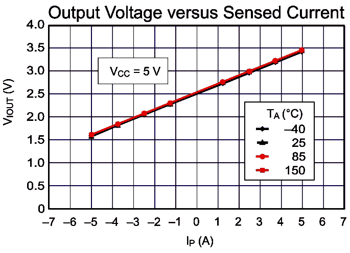
The curve below shows the nominal sensitivity and transfer characteristics of the ACS712-05B sensor powered with a 5.0V supply. The drift in the output is minimum for a varying operating temperature, which is attributed to an innovative chopper stabilization technique implemented on the chip (read ACS712 datasheet for detail).
|
|
|
| Output voltage vs sensed current of ACS712-05B at 5.0 V power supply and varying temperature. |
Summary
This article briefly described the ACS712 current sensor and its basic features. Continue reading the second part of this discussion to see how to use it with a PIC microcontroller to measure DC current.
Part 2 - Interface the sensor with a PIC microcontroller
