Zero-crossing detectors synchronize the turn-on time of an ac switch with the zero-voltage condition and are often used to reduce in-rush current and commutation noise. The zero-crossing detectors described here control triacs, but they’re also suitable for other applications.
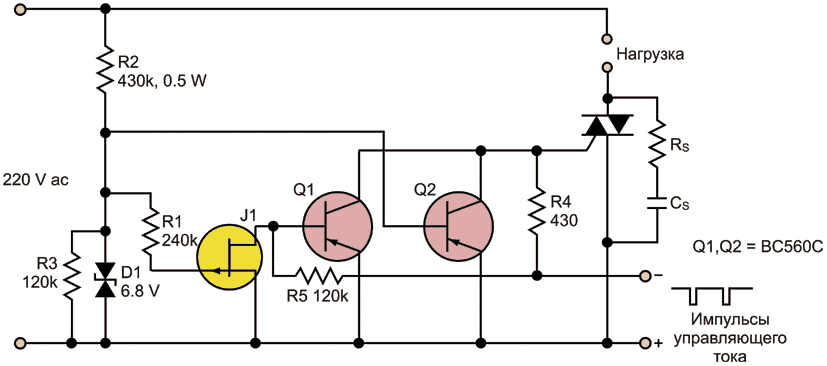
Many triacs must be triggered in the three first quadrants. The circuit in Figure 1 can drive these devices in the second and third quadrants, when the gate current is negative. In this circuit, Q1 is on during the positive ac half cycle – that is, when the upper ac rail is positive. Q2 is on during the negative half cycle. The transistors are off only near zero-ac level where the triac’s triggering may occur.
 |
|
| Figure 1. | This zero-crossing detector circuit generates the control pulses needed to turn on triacs that require negative pulses for switching. |
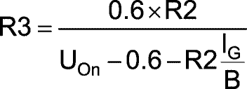
To reduce ac power consumption, all the transistors (bipolar-junction devices) should deliver sufficient gain so:

where B is the gain of Q2, IG is the triac’s minimal effective gate current (the sensitivity of the triac), and UOn is the maximum ac level when triggering is allowed. Once the value of R2 is determined, you can calculate the value of R3:

While the ac value is near zero, negative current pulses flow through the triac’s gate triggering it, because neither Q1 nor Q2 is shunting the triac’s gate circuit. Eventually, the main current is established when it exceeds the triac’s minimal latch current. If the triac is not triggered during this period, then the absolute value of the ac will exceed UOn and Q1 (or Q2) will turn on, preventing triggering.
The more difficult task for this circuit is to control the gate current for the negative triac during the positive ac half waves. The p-JFET, J1, helps with this job by providing the required voltage shift and minimizing ac losses. J1 is on near the ac zero point, so Q1 goes off.
Then, as the ac goes more positive and reaches the value of UOn, J1 goes off and Q1 goes on. The bipolar Zener diode, D1, protects the p-n junctions of J1 and Q2. The diode’s capacitance (200 to 400 pF) together with R2 comprises a low-pass filter that blocks possible ac spikes. R1 limits potentially harmful direct current through J1’s gate.
An alternative for this rather complicated design is to use a common-base pnp input cascade combined with a common-collector npn cascade. But a circuit used for direct control of a triac requires a quite high current gain that is hard to obtain without sacrificing ac power consumption.
The problem is that the current level through R2 is very close to the level of the emitter current in the common-base cascade, which can’t be very low without reducing the gain. As a result, we opted for the JFET front-end solution. The main requirement for the low-power p-JFET is a rather low cutoff voltage – less than 2 V, but the lower the better.
To ensure there are no problems with latch current, you may have to use long control pulse trains or dc gate current. The triac used had an IG of less than 20 mA. R4 is a safety net that protects the transistors from excessive control current. RS and CS form a snubber network, which can be omitted, depending on the load and kind of triac used.
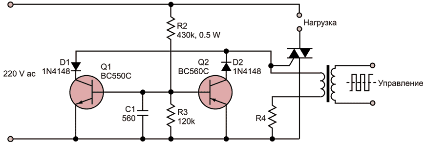
Most triacs can be triggered by either a positive or a negative voltage applied to the gate. For those, the circuit shown in Figure 2 can be used. This circuit offers bipolar control and is better suited for use with a transformer. Note that the optional snubber is omitted in this circuit.
 |
|
| Figure 2. | Designers can use this version of the zero-crossing circuit for triacs that can be triggered by either a positive or negative voltage. This circuit is well-suited for transformer control. |
