There are several ways to read multiple switch inputs using a reduced number of microcontroller-unit (MCU) pins. For example, you can use an analog MCU pin to read multiple switches by assigning a unique voltage to each switch through a resistor network, or you can use a one-wire device, such as the Maxim DS2408 8-channel addressable switch.
The first method has several disadvantages: The MCU has to have an ADC function, debounce wait times reduce the polling rate, and an error results if the switch is opened during the ADC sampling time. The second method also has the drawback of comparatively low speed; it uses 1-wire communication, which requires continuous polling; and each poll generates an 8-bit data sequence relevant to switch positions.
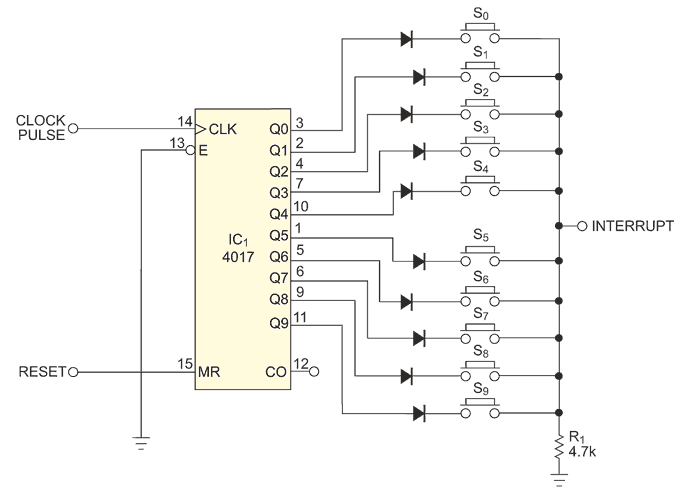
This Design Idea describes a method for reading multiple pushbuttons or open/closed switches using only two digital I/O pins and a timer interrupt of the MCU (Figure 1). Optionally, a third I/O pin can be assigned to periodically reset the CD4017 (a cascadable decoded 1-of-10 Johnson counter) for reliable operation should an EMI or ESD event occur that could falsely clock the counter, or you can use the circuit shown in Figure 2 and retain the two-pin feature. The diodes isolate the counter outputs in the event that two or more switches are closed at the same time. You can increase the number of switches connected by cascading multiple CD4017 ICs using a carry-out signal (pin 12) and a clock signal (pin 14).
 |
|
| Figure 1. | You can easily expand this circuit to many more than 10 switches, yet still use only two MCU I/O pins, by cascading multiple CD4017 counters through their carry-outs to the following enables. |
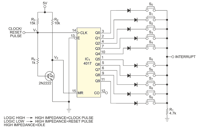
Reliable operation following the initial power-up reset depends on the CD4017 counter’s remaining synchronized with the MCU counter. This synchronization can be upset by an ESD or EMI event such as a nearby cell phone, so it would be wise to include in the firmware a periodic hardware reset to the CD4017 to keep the counts synchronized. Figure 2 shows how you can do this without having to use a third MCU pin.
 |
|
| Figure 2. | You can add three resistors and a transistor to implement the occasional synchronizing reset without using a third I/O pin. |
For this function, you use the MCU’s ability to keep its I/O pin in three different states: high, low, and, by temporarily changing the pin to an input, high impedance.
In the logic-high state, transistor Q1 turns on through R4, making the voltage on V1 logic high and the voltage on V2 below the logic-low level. This sets the clock pin to a logic high while keeping the reset pin at a logic low.
In the logic-low state, transistor Q1 turns off, making the voltage on V1 logic low and the voltage on V2 above the logic-high level. This sets the reset pin to logic high while keeping the clock in the logic-low state.
In the idle high-impedance state, transistor Q1 is turned on through R3 and R4, making the voltage on V1 and V2 below the logic-low level. This sets both the clock and reset pins of the CD4017 to a logic-low state.
To send a clock edge, therefore, change the state in the following manner: high impedance > logic high > high impedance. Likewise, to reset the CD4017, change the state as follows: high impedance > logic low > high impedance.
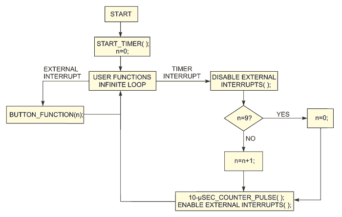
The flowchart in Figure 3 is for an all-pushbutton system and functions as follows: At the start, the MCU sets a counter variable to 0 and starts an interrupt-enabled timer, which is set to overflow and interrupt at 1-msec intervals. In the timer-interrupt routine, several tasks are carried out: External interrupts are disabled; the counter variable is incremented by 1; a 10-μsec clock pulse is sent to the CD4017; and the external interrupt is enabled.
 |
|
| Figure 3. | This flowchart displays the process for reading an all-pushbutton system. Only one button at a time should be pressed. |
As the MCU clocks the CD4017 every 1 msec and increments the counter variable by 1 if its value is less than 9, the CD4017 output corresponding to the counter-variable value goes to logic high from logic low; that is, if the counter-variable value is 2, then the decoded 2 output of the CD4017 (pin 4) is at logic high while all other outputs are at logic low. At this time, if the user pressed pushbutton S2, it would send a logic-high signal to the external interrupt pin of the MCU. Pressing any other button does not generate external interrupts, because all other outputs of the CD4017 are in the logic-low state.
When the MCU receives the external interrupt, it gets the current counter-variable value (which is 2) from its memory, identifies the pressed button as S2, and thus carries out the functions relevant to S2. When the counter variable reaches 9, it is set to 0 through the software, as the CD4017 also resets automatically at the 10th pulse.
 |
|
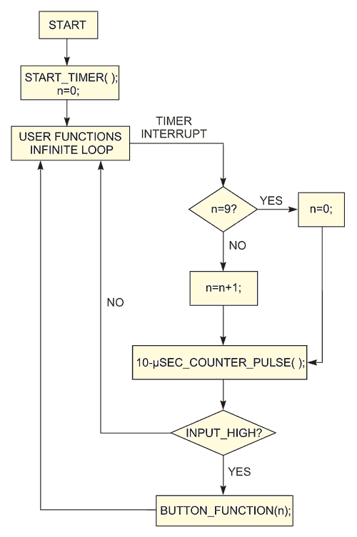
| Figure 4. | When non-momentary toggle switches are used, you can decode multiple combinations of switch closures by checking the state of the interrupt input. |
Note that only one button at a time should be pressed; if two consecutive buttons are pressed together, there may not be enough dropout time between successive counter states for the interrupt edge to register. You can resolve this issue by using the flowchart shown in Figure 4.
Additional materials:
