Part 1 - Schematic
The software drivers
My previous Nokia QVGA reverse engineering efforts that you can find documented extensively on this site have left me with a flexible and expandable driver that will make a good base from which to add support for this new adaptor.
The driver code is separated into access modes and panel drivers that are bound together with a graphics library at compile-time by using C++ templates. To support this new adaptor I will need to write at least one new access mode and as many panel drivers as are required to support the panels that I own.
Let’s get started by taking a look at the 16-bit XMEM access mode.
The 16-bit xmem access mode
The XMEM interface built into the Arduino Mega MCU is designed to provide access to external memories with a 16-bit address bus and an 8-bit data bus. It just so happens that the protocol for accessing these memories is close enough to the 8080 protocol required by the LCDs that I can sometimes use it successfully. I say ‘sometimes’ because external factors such as the panel timing parameters do come into play.
So, when the Arduino Mega wants to write to an external memory it does the following:
- ALE is driven high.
- It drives the 16-bit address on to the bus where the lower 8 bits are multiplexed with the data lines.
- ALE is driven low, locking in the lower 8-bits of the address.
- It pules the WR line from high to low and to high again. Data is transferred on the rising edge of the pulse.
I can make use of this sequence to transfer 16-bits to the LCD in a single transaction that also includes the RS (register/data select) line. I will use the lower 8-bits of the 16-bit address to transfer the lower 8-bits of LCD data. I will use address line A8 to hold the RS signal and I’ll use the 8 data lines to transfer the upper 8-bits of LCD data. I will also set bit 15 of the address so that I’m guaranteed to be in the external memory range and will not collide with the internal 8Kb of SRAM.
Let’s take a look at the pinout for this access mode:
| Arduino | Port | Function |
| 22 | PA0 | D0/D8 |
| 23 | PA1 | D1/D9 |
| 24 | PA2 | D2/D10 |
| 25 | PA3 | D3/D11 |
| 26 | PA4 | D4/D12 |
| 27 | PA5 | D5/D13 |
| 28 | PA6 | D6/D14 |
| 29 | PA7 | D7/D15 |
| 35 | PC2 | /RESET |
| 37 | PC0 | RS |
| 39 | PG2 | /CS |
| 41 | PG0 | /WR |
Initialising the XMEM interface is a simple matter of writing the correct values to the two XMEM registers. The XMEM pins 30..34 (PC3..PC7) are free’d up for GPIO.
inline void Xmem16AccessMode::initialise() {
      // set up the reset pin
      pinMode(RESET_PIN,OUTPUT);
      digitalWrite(RESET_PIN,HIGH);
      // set up the xmem registers
      // free PC3..PC7 for user GPIO
      XMCRB=_BV(XMM1) | _BV(XMM2);
      // enable xmem, no wait states      XMCRA=_BV(SRE);
  }
Because performance is absolutely paramount I wrote the data and command output functions in AVR assembly language.
inline void Xmem16AccessMode::writeData(uint8_t lo8,uint8_t hi8) { // this is equivalent to: // *reinterpret_cast <volatile uint8_t *>(0x8100 | lo8)=hi8; // this method costs 5 clock cycles __asm volatile(" ldi r27,0x81n
t" " mov r26,%0
n
t" " st X,%1
n
t" :: "d" (lo8), "d" (hi8) : "r26", "r27"); }
In AVR assembly language the combination of r26 and r27 make up a 16-bit X register that we use in the above code to send the 8-bit data value to the external memory. It’s also helpful that r26 and r27 are free for use in inline assembly code without fear of colliding with code emitted by the C++ compiler. Nevertheless I do declare them in the ‘clobber’ list at the end of the __asm section.
The method used to write a command is almost the same, except bit A9 is set to zero:
inline void Xmem16AccessMode::writeData(uint8_t lo8,uint8_t hi8) { // this is equivalent to: // *reinterpret_cast <volatile uint8_t *>(0x8000 | lo8)=hi8; // this method costs 5 clock cycles __asm volatile(" ldi r27,0x80n
t" " mov r26,%0
n
t" " st X,%1
n
t" :: "d" (lo8), "d" (hi8) : "r26", "r27"); }
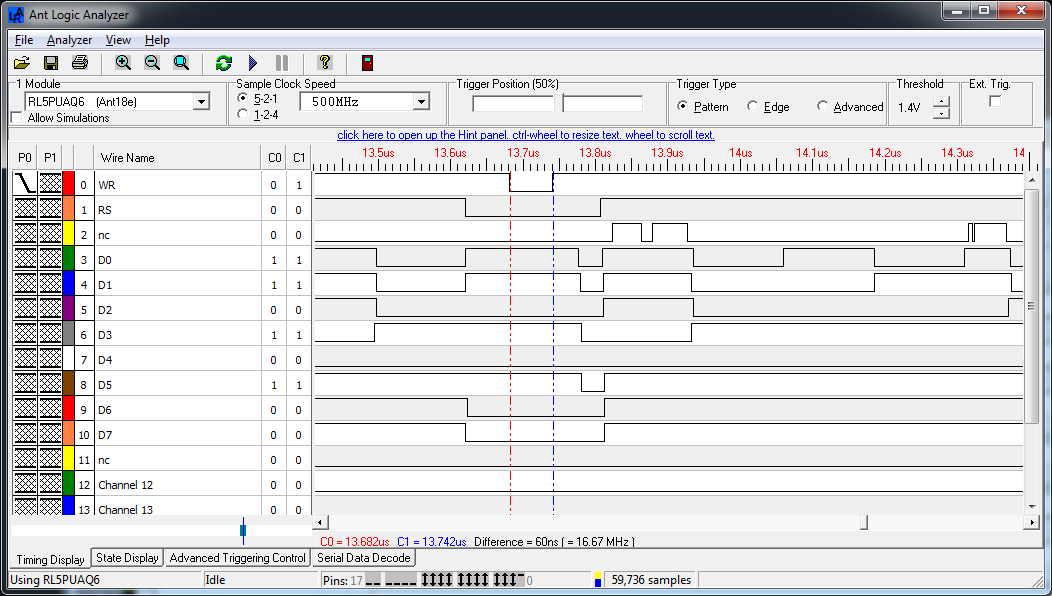
To see this access mode in action we need a logic analyser so I hooked up the output of the adaptor to my Ant18e and captured the lower 8 data lines, RS and WR.
 |
|
| Figure 8. | 16-bit xmem access mode: Captured the lower 8 data lines, RS and WR. |
I can see from the section between the two timing markers that the AVR core pulses WR for exactly one clock cycle.
Some of the panels that I have are not happy with the tight timings provided by the XMEM interface, even when I add some address and data hold cycles so for this reason I decided to branch out and build an optimised GPIO access mode. I’m glad that I did because in some areas the optimisations that I created resulted in a huge performance increase.
The 16-bit gpio access mode
The 16-bit GPIO access mode emulates the automatic operation of the XMEM interface by using ordinary GPIO. There are advantages and disadvantages to this approach. Single writes are going to be a few cycles slower than the XMEM interface but for multiple writes of the same value I can optimise heavily to create a routine that will outperform anything else as long as the panel supports 16-bit (64K colour) mode. The other advantage is that I’m not restricted to the XMEM pins and I could even get it to work on the ordinary 32Kb Arduino.
Gpio16LatchAccessModeXmemMapping is a template that takes a type containing my port and pin mappings as its parameter. For example, using the same ports and pins as Xmem16AccessMode I declare this type:
struct Gpio16LatchAccessModeXmemMapping { enum { // ports are the I/O index, not the physical address PORT_DATA = 0x02, // PORTA PORT_WR = 0x14, // PORTG PORT_RS = 0x08, // PORTC PORT_ALE = 0x14, // PORTG PORT_RESET = 0x08, // PORTC // pins are the 0..7 port index, not the arduino numbers PIN_WR = PIN0, PIN_RS = PIN0, PIN_ALE = PIN2, PIN_RESET = PIN2 }; };
The Gpio16LatchAccessMode template looks like this. You can see that I also provide a concrete instantiation of the template using a typedef for easy use.
template<typename TPinMappings>
 class Gpio16LatchAccessMode {
        protected:
          static uint8_t _streamIndex;
          static void initOutputHigh(uint8_t port,uint8_t pin);
        public:
          static void initialise();
          static void hardReset();
          static void writeCommand(uint8_t lo8,uint8_t hi8=0);
          static void writeCommandData(uint8_t cmd,uint8_t data);
          static void writeData(uint8_t lo8,uint8_t hi8=0);
          static void writeMultiData(uint32_t howMuch,uint8_t lo8,uint8_t hi8=0);
          static void writeStreamedData(uint8_t data);
    };
      typedef Gpio16LatchAccessMode<Gpio16LatchAccessModeXmemMapping> DefaultMegaGpio16LatchAccessMode;;
I’ll skip the initialise method because I’m sure you’re not particularly interested in code that just sets the direction and level of GPIO pins. Let’s get straight on to the writeData() and particularly the writeMultiData() methods. Firstly, writeData(), the method that writes out a single value:
template<class TPinMappings> inline void Gpio16LatchAccessMode<TPinMappings>::writeData(uint8_t lo8,uint8_t hi8) { __asm volatile( " sbi %1, %5n
t" // ALE = HIGH " out %3, %7
n
t" // PORTA = lo8 " sbi %2, %6
n
t" // RS = HIGH " cbi %1, %5
n
t" // ALE = LOW " out %3, %8
n
t" // PORTA = hi8 " cbi %0, %6
n
t" // /WR = LOW " sbi %0, %6
n
t" // /WR = HIGH :: "I" (TPinMappings::PORT_WR), // %0 "I" (TPinMappings::PORT_ALE), // %1 "I" (TPinMappings::PORT_RS), // %2 "I" (TPinMappings::PORT_DATA), // %3 "I" (TPinMappings::PIN_WR), // %4 "I" (TPinMappings::PIN_ALE), // %5 "I" (TPinMappings::PIN_RS), // %6 "d" (lo8), // %7 "d" (hi8) // %8 ); }
Straightforward stuff. We just bit-bang the 8080 protocol with the additional overhead of the latch programming.
Now, it’s very common in graphics libraries to write out solid blocks of colour. Whether you’re clearing the screen, drawing rectangles or just straight lines it all comes down to setting an ‘output window’ on the display and then pumping out pixels.
The writeMultiData() method takes advantage of the fact that you only need to set the data and RS lines once and then you can toggle the /WR line as often as you need to in order to write out your block of pixels. This technique was first suggested to me by Andrew, the author of this instructable. Here’s my take on the method.
This is how it works.
- We program RS and set up the 16 data lines.
- If interrupts were enabled when we came in then I disable them. As well as ensuring a consistent timing this ensures that an ISR cannot change the port values that I set up in (3).
- The port holding WR is read and I cache this value in registers with the WR bit set and reset.
- If there are fewer than 40 pixels to write then go to step 7.
- Write out 40 pixels using consecutive out commands. This achieves an 8 megapixel/second fill rate.
- Subtract 40 from the pixel counter and if more than 40 remain then go back to step 5.
- Calculate an indirect jump into the trailing 39 out commands that will fill the remaining pixels and use ijmp to go there.
- If we disabled interrupts then restore them.
The number 40 was chosen somewhat arbitrarily as a trade off between flash memory usage and performance. I tried values of 10, 20, 30, 40 and stopped there as the increase in speed was getting smaller and smaller to the point of irrelevance.
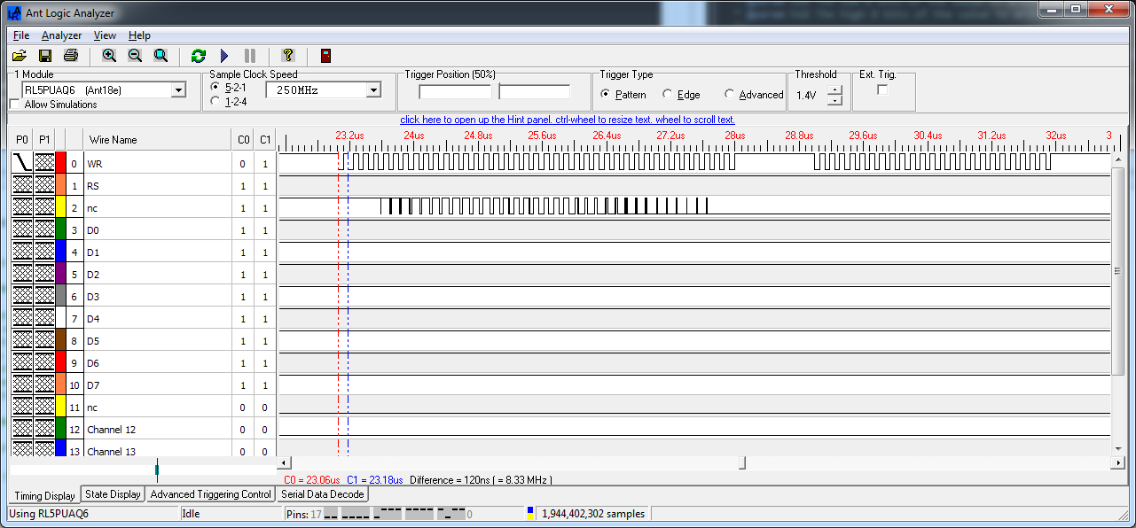
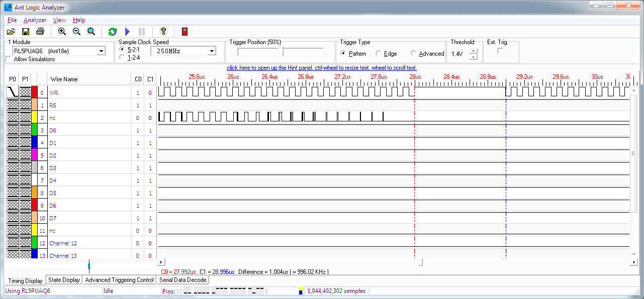
Once again, to see the effect of this code a logic analyser is required. Hooking up the trusty Ant18e yielded these captures (Figure 9, 10).
 |
|
| Figure 9. | The effect of the optimised /WR toggling. As expected we are achieving a fill rate of 8 megapixels/second. |
 |
|
| Figure 10. | Capture shows how much overhead is added by the code that subtracts 40 from the total and jumps back to execute the next block of 40 pixels. It is 1 microsecond. |
So is it worth this hand-optimisation? Yes it definitely is. In the following sections where I show the panel drivers that I’ve written, the accompanying videos are all running this driver. You can see how fast the screen clearing, rectangle drawing, gradient drawing and solid ellipse drawing operations are for yourself.
Part 3 - Optimization and Driver Configuration