There are many TFT modules available on the market that are designed to connect directly to an MCU to provide a full colour graphical display, just search ebay for “tft module” to see what I mean.
Unfortunately for Arduino users the majority of these modules expose a 16-bit interface and are designed to be connected to ARM devices. The way I see it there are two problems to be solved here in order to allow them to be connected to an Arduino. Firstly, they are always designed to be run at 3.3V and secondly the 16-bit data bus uses up a ton of GPIO pins (Figure 1).
 |
|
| Figure 1. | A Generic Optimized 16-bit LCD Adaptor for the Arduino. |
I’m going to present a combination of hardware and software that solves both of those problems and also shows how you can achieve extremely high performance with a few driver optimisation tricks.
The hardware adaptor
I decided to design an adaptor that would feature 5V to 3.3V level conversion as well as a latch that would allow me to reduce the pins required by the data bus from 16 to 8 at the expense of an additional pin for controlling the latch. A total saving of 7 pins over the simplistic solution.
How does the latch work?
The latch works sort of like a small memory. In ‘transparent’ mode signals pass right through it and come straight out the other side. When you flip to ‘latched’ mode the latch ignores its inputs and continues to output the last values it received on those inputs.
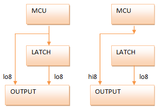
I can use these properties of the latch to push out two 8-bit values in sequence and have the latch ‘expand’ them to 16-bits.
|
|
|
| Figure 2. | Two phases of the operation of the latch. |
The diagram (Figure 2) shows the two phases of the operation of the latch. In the first phase I push out the low 8-bits which gets routed through and around the latch to occupy both the low (which I want) and the high (which I don’t want) bytes of the output. In the second phase I lock the latch and then push out the high 8-bits. The latch ignores this new data and so the only route is around the latch into the correct position in the outputs.
Another advantage of the latched design is that it dovetails nicely with the external memory (XMEM) peripheral that comes built in to the Arduino Mega 1280 and 2560. With a little bit of clever code I should be able to use the XMEM interface to drive the LCDs.
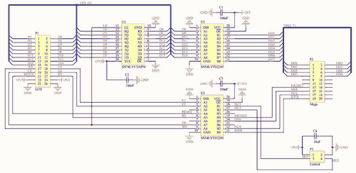
The schematic (Figure 3)
 |
|
| Figure 3. | A Generic Optimized 16-bit LCD Adaptor for the Arduino: Schematic Diagram |
The schematic pulls together the level conversion, latch, a connector designed to directly fit the Arduino Mega and an output connector for the 16-bit LCD. I’ll explain each sub-section of the schematic here.
The Arduino Mega Connector
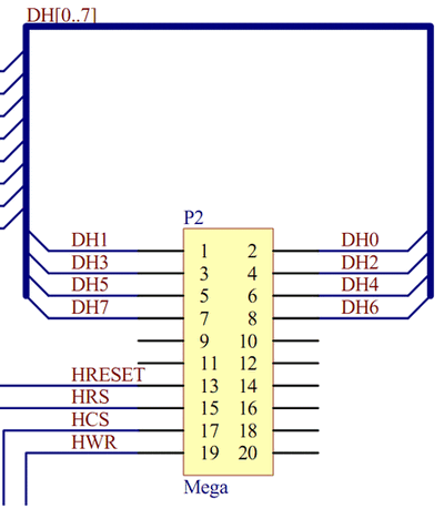
This a 10×2 male pin header with pin assigments designed to match the Arduino Mega’s XMEM interface that is exposed in the block of pins starting at 23 (Figure 4). The letter ‘H’ in the net designators indicates that these are high level 5V signals. I should probably have used ‘T’ for TTL but there you go.
 |
|
| Figure 4. | A 10×2 male pin header with pin assigments designed to match the Arduino Mega’s XMEM interface |
The data and control signals are all there, including CS (chip-select) that I map to ALE (address latch enable) on the XMEM interface even though this signal is rarely required by the LCD panels and can usually be just tied to ground.
The level converters
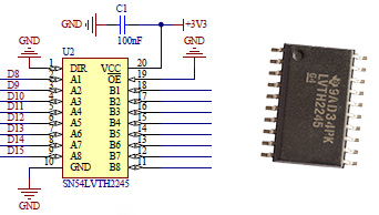
The SN54LVTH2245 octal bus transceiver from Texas Instruments is an ideal choice for level conversion in this design (Figure 5). The propagation delay at 3.3V is around 2ns which is very fast. The inputs and outputs are on opposite sides of the package which simplifies routing and it’s easy to find the device on the market.
 |
|
| Figure 5. | SN54LVTH2245 octal bus transceiver from Texas Instruments. |
The latch
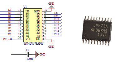
The SN74LV573APW transparent D-Type latch, again from Texas Instruments, satisfies the speed requirements imposed by the XMEM interface and is easy to find on the market (Figure 6). Latches, like bus transceivers are readily available in all shapes and sizes and there’s nothing to stop you using different parts as long as the specifications are similar to these.
 |
|
| Figure 6. | SN74LV573APW transparent D-Type latch. |
The control header
This is a 2×2 pin male header that I’ll use to provide the vital power and ground supplies from the Arduino board. The two ‘user’ inputs U1 and U2 can be used to convert any arbitrary output signal from the Arduino from 5V down to 3.3V. I added these because I had some unused ports on the level converters and it did seem a shame to waste them. Later on you will see how I use one of these to provide a PWM backlight control to the LCD panels.
The output connector
This connector provides the output signals for the LCD. In my design I’ll be using a right-angled male header to simplify the rats nest of interconnecting wires that need to be connected here.
As well as the output signals there are pairs of power and ground outputs. You can’t have too many of those!
The PCB design
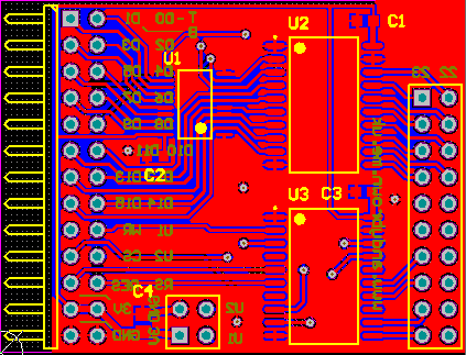
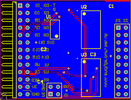
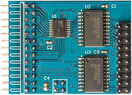
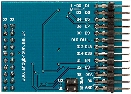
Manually routing the board didn’t present any real challenges and I was able to fit the whole design into a 45mm by 35mm PCB. Thankfully this time I’d remembered to check that the level converters had inputs and outputs on opposing sides of the package instead of adjacent to each other (Figure 7).
 |
|
 |
|
 |
|
 |
|
| Figure 7. | A Generic Optimized 16-bit LCD Adaptor for the Arduino: PCB Design. |
My procedure for building a PCB with surface mount components remains unchanged. Firstly I tin all the pads with a soldering iron and some highly active flux that makes for easy drag soldering across the small IC pads. Then I thoroughly clean all the flux residue off the board because the acids can attack the board over the long term.
Now the pads are tinned I use a hot-plate to reflow the ICs into place and touch up the reflowed joints afterwards under a binocular microscope. The discrete components are then reflowed into place with my Aoyue 852A hot air gun and finally the pin headers are soldered into place with an ordinary soldering iron. The final touch is to wash the boards in hot soapy water and leave to dry for 24 hours.
Now I’ve got something that I can play with it’s time to see if I can come up with some driver software that will do it justice. Something tells me I can…
Downloads
Schematic Diagram and PCB Design (PDF) - download
Part 2 - Software
Part 3 - Optimization and Driver Configuration
