Deivaraja Ramasamy
EDN
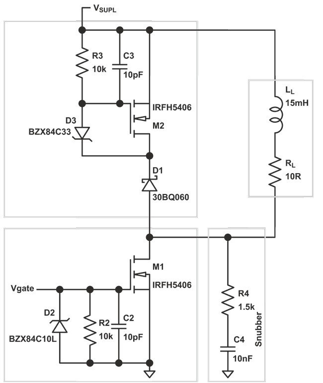
This Design Idea is able to turn off inductive loads at a very fast rate. When connected to a load (here 15 mH + 10 Ω), the modified freewheeling path in the clamping circuit based around M2 reduces the turn off time to 450 µs. A simple freewheeling diode in place of the clamping circuit takes about 4 ms to turn off the load.

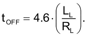
In a diode-freewheeled circuit, the voltage across the load increases by just the diode forward conduction voltage, and so the current decays as a function of e-t. If the off current is defined as 1% of the saturation current, the turn-off time with a typical freewheeling diode can be calculated from the below expression:

With the modified circuit, the turn-off time is reduced by increasing the clamp voltage. The circuit uses the same configuration of N-channel power MOSFETs for both the low-side conduction and the clamping.
The resistors R2 and R3 serve to discharge the gate of the transistors to turn them off in case of a power failure. The zener diode D2 limits the gate voltage at M1. C2 and C3 serve to reduce the dVDS/dt, to avoid latch-up. The gate of M1 is connected to the control signal to turn off or on the load. M2, the clamping transistor, conducts whenever the voltage at the load is about 50 V. Diode D1 serves to block the conduction of the body diode of M2. Diode D3 increases the clamping voltage, so that there is a fast turn-off. The turn off time is given by the equation:
![]()
Note that the turnoff time linearly decreases with VD3, the zener clamp voltage of diode D3. D3’s voltage is selected so that no avalanche events occur at M1 or M2. The transistors M1 and M2 IRFH5406 have a VDS(max) of 60 V. R4 and C4 form a snubber circuit to damp the oscillations caused by resonances due to the inductive load along with the parasitic capacitances of M1 and D1.