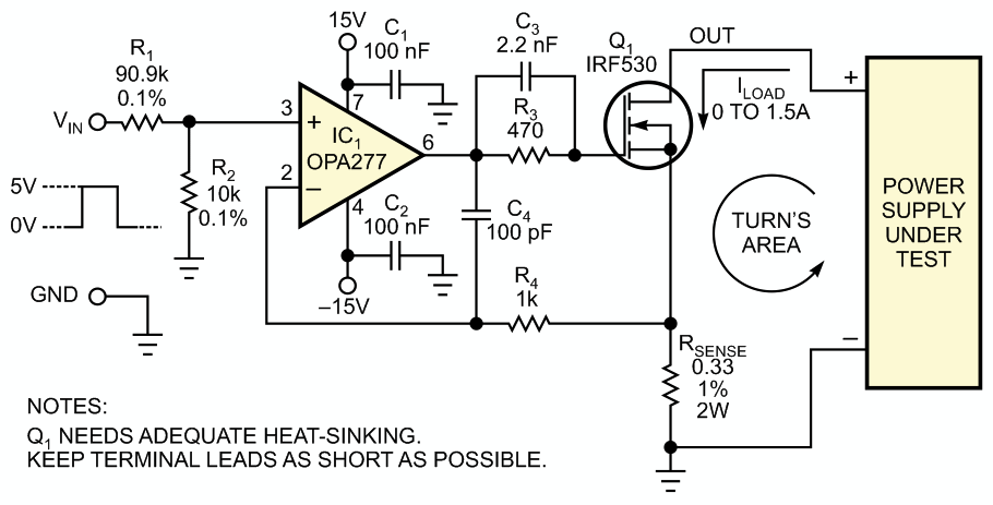
To discover potential power-supply problems, you must run dynamic and static tests. This simple current sink tests low- to medium-power supplies and voltage sources. In this application, the current sink can draw current of 0 to 1.5 A for an input-voltage range of 0 to 5 V with a supply voltage as high as 20 V. The basis of the circuit is precision op-amp IC1, an OPA277 from Texas Instruments, which features a maximum input-offset voltage of only 100 µV, maximum input-bias current of 4 nA, and low drift over the temperature range of –40 to +85 °C (Figure 1). The op-amp IC compares its positive input voltage with the voltage across sense resistor RSENSE.
 |
|
| Figure 1. | This simple current sink allows you to test both the static and the dynamic behavior of power supplies. |
IC1’s output drives an enhancement-mode N-channel power-MOSFET, Q1, an STMicroelectronics IRF530, such that the voltage across the sense resistor equals the positive-input voltage. The voltage across the sense resistor is proportional to the load current from the power supply under test and is independent of its output voltage. Q1 features a maximum current of 14 A at a case temperature of 25°C with drain-to-source voltage of 100 V, low gate charge, and maximum on-resistance of 0.16 Ω at a gate-to-source voltage of 10 V and a drain current of 7 A.
The MOSFET can dissipate a finite amount of maximum power – to 30 W with the heat sink’s thermal resistance of 1°C/W or less and an ambient temperature of 40 °C or less in still air. The maximum power depends on the thermal resistance of the heat sink you use and the ambient temperature, so, when you increase the supply voltage, you must accordingly reduce the load current. By pulsing the input voltage, you can increase the supply voltage to several 10s of volts because the average power dissipation is lower and depends on the average load.
The precision resistive divider, R1 and R2, allows you to convert the input-voltage range of 0 to 5 V into 0 to 0.495 V at the positive input of IC1, resulting in an output-current range of 0 to 1.5 A. In addition, the values of resistors R1 and R2 provide 100 kΩ of input resistance, which is adequate for most voltage-function generators having a source impedance of 50 or 75 Ω, allowing them to drive the circuit’s input without using an input-op-amp buffer.
Analyzing the circuit yields the following relationships:
ILOAD = GVIN,
with

where
G is the conductance,
α is the attenuation factor:

You can change the attenuation factor of the input-voltage divider to adjust the upper limit of the output current to several amperes, which allow you to test low-voltage power supplies with high output current.
Capacitors C3 and C4 and resistors R3 and R4 ensure loop stability, yielding a circuit with a rise time of 1.4 µsec for an input step voltage of 0 to 5 V. So, you can test power supplies in either static conditions, applying a dc input voltage, or dynamic conditions, applying, for example, a pulsed input voltage to simulate fast load transients. Also, you can test power supplies or voltage sources as low as 1 V because of the low channel resistance of Q1 and the RSENSE resistor; the lower limit is
(1.5 A) × (RSENSE + RDS(ON)) = 735 mV,
where RDS(ON) is the on-resistance.
You can also test multiple regulated outputs of power supplies such as a –5 or a –12 V supply voltage. In this case, you must connect the ground of the power supply to the output of the current sink – that is, the drain terminal – and the negative output with the ground of the circuit. For accuracy, when you perform dynamic tests, such as load regulation, recovery time, and transient response, you must take care when connecting the power supply under test with the circuit to reduce the turn’s area. The pulsed load current produces radiated emissions, which are proportional to this area, to the value of the current, and to the square of the current frequency, and they may disturb the circuit itself and the measuring equipment.
