Alex Rysin
Electronic Design
This idea analyzes the reason that a capacitively coupled load may result in a clipped negative output, and shows the conditions that must be met to avoid this undesired situation.
An engineer asked me for help when he encountered what appeared to be strange phenomenon while testing a prototype circuit in the system. He saw “mysterious” clipping distortion of the signal at the output of his emitter follower. He told me that he checked this follower with a much-heavier (smaller-value) resistive load than the actual load, but did not see any visible distortions. However, when he connected his prototyping board to the system, there was significant clipping of the signal at the bottom.
Looking at the schematic, I saw that the resistive input of the next device is decoupled from his follower by a large capacitor. I explained to him the reason for the problem. I also realized that, unlike with a resistive load when the possibility of clipping is fairly obvious, the problem with a capacitively coupled resistive load can be easily overlooked during the design.
A one-transistor emitter follower can source as much current to the load as the load needs, within its transistor’s limits. However, the transistor cannot sink current. This may cause clipping distortions of the output signal when the follower is ac-coupled to a resistive load, for reasons which are sometimes not obvious.
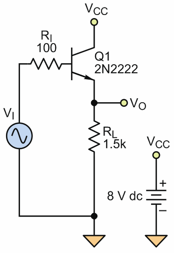
First, look at the simple NPN emitter follower (Fig. 1a) and its possible obvious clipping distortions. Positive clipping to VCC on the output will occur if a large input signal exceeds VCC by about 0.7 V, turning on the base-collector junction of the transistor Q1 (here, a common 2N2222). That junction works like a diode above the clipping point, shunting the input signal to VCC. If this diode's current is not limited by an appropriate value of input resistor RI, the transistor may be damaged.
 |
|
|
а) |
|
 |
|
|
b) |
|
 |
|
|
c) |
|
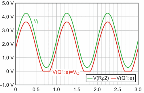
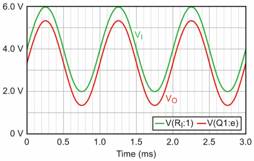
| Figure 1. | The analysis uses a basic emitter-follower circuit, using the ubiquitous 2N2222 transistor (a). As the input signal (green, top) drops below VBE, the output signal (red, bottom) is clipped to 0 V (b). There is no clipping distortion on the output signal with VOFF = 4 V (c). |
Negative clipping occurs during the negative swing of the input signal if the input level at the base of the transistor becomes less than about 0.7 V (the VBE of the transistor). In this case, the base-emitter junction of the transistor becomes reverse-biased, its emitter current (IE) drops down to zero, and the transistor turns off. This causes clipping of the output signal to zero at its bottom until the input signal returns the transistor to the normal mode.
Close to the clipping point, emitter current IE is low, and the follower increases its total harmonic distortion (THD) level. In the case of a sinusoidal input signal, to prevent this obvious clipping:
| (1) |
where VAMPL is the peak amplitude and VOFF is the dc offset voltage of the sine-wave input source.
The described clipping is illustrated using PSpice transient analysis of the circuit, with the ac input source set for VAMPL = 2 V, VOFF = 2.3 V and frequency of 1 kHz. In this case, VI_MIN = 0.3 V and the transient analysis shows a clipping at the bottom of the output signal (Fig. 1b).
Figure 1c shows results of the same circuit simulation with VOFF = 4 V, which gives a 1.3-V margin above the clipping level. Now the transient analysis doesn’t show clipping and other noticeable distortions of the output signal. Also, the Fourier analysis in the simulation profile shows THD of 0.143% in the output file.
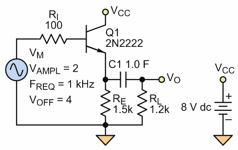
Increasing the follower's load produces a similar result. For example, even with RE = 0.5 kΩ in the circuit of Figure 2a (which is one third of the RE used in the simulation), there aren’t any noticeable changes in the graph and only slightly increases of THD to 0.145% from 0.143%.
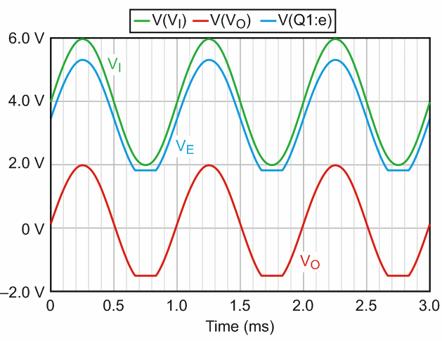
Next, connect the ac-coupled load resistor to the follower. The value of the decoupling capacitor C1 is chosen as large enough (1.0 F) so as to not contribute to possible distortions of the output signal at the end of the transient process. At first glance, you would expect the same result of the simulation as for the circuit in Figure 1, but without a dc component on RL. However, the transient analysis (Fig. 2b) shows a significant clipping of the output signal and on the emitter of the transistor.
 |
|
|
а) |
|
 |
|
|
b) |
|
| Figure 2. | An ac-coupled resistive load was added to the original emitter-follower circuit (a). Inserting the decoupling capacitor between RE and RL causes significant clipping distortion of the input signal (green, top), seen at the emitter of the transistor (blue, middle) and at the follower's output (red, bottom) (b). |
There’s a simple explanation for this non-obvious result. In the steady state, C1 is charged to the dc level of Q1’s emitter. During the positive half-cycle of VIN, Q1's emitter current splits and goes to RE and RL (IRE and IRL, respectively). The maximum level of the emitter current IE_MAX is:
![]()
However, during the negative half-cycle of VIN, while IRE is still directed out of transistor Q1, thus decreasing its value, IRL is directed back to Q1 and is subtracted from IRE.
If the result of this subtraction is negative, IE_MIN drops to zero and the output signal suffers from clipping.
The reason IRL is directed back to Q1 also isn’t obvious. In the steady state, C1 is fully charged. The dc voltage on its left side is VE, which is higher than the absolute voltage at minimum AC signal (VAC_AMPL = 2 V) and in this case is equivalent to 4 – 0.7 = 3.3 V. The capacitor’s dc level on the right side is zero.
Consequently, during the negative cycle of the ac signal, the voltage across RE follows the negative wave of the input signal, but is always positive because of the bias. The RE component in the combined current equals the voltage at the emitter of Q1/RE > 0. Output voltage VO on the top of RL also follows the negative wave of the input signal, but it has zero dc bias. It’s also negative for the negative wave. In this region, it changes from zero to negative VAMPL, which causes the current through RL to go in the opposite direction. IRL is always less than 0.
To prevent the clipping problem, IE_MIN should be always greater than zero:
![]()
or
| (2) |
Thus, to avoid clipping in the one-transistor emitter follower with an ac-coupled resistive load, the three variables of Equation 2 should comply with the following constraints:
![]()
or

or
![]()
and also, from Equation 1:
![]()
References:
- Alan B. Grebene, Bipolar and MOS analog integrated circuit design, Wiley - Interscience Publications, John Wiley & Sons.
- Douglas Self, Small Signal Audio Design, Focal Press, 2010.
- P. Horwitz, Winfield Hill; The Art of Electronics, Second Edition, Cambridge University Press, 1989.
