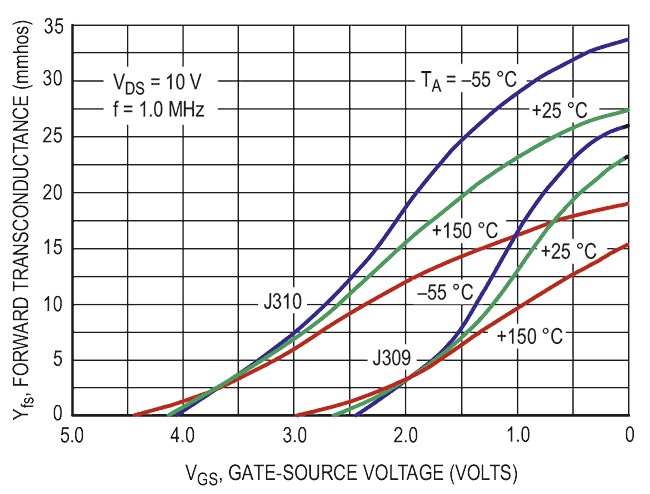
While JFETs are excellent devices for low-cost high-input impedance amplifiers, they do suffer from temperature-dependent gain drift (Figure 1). This problem can be ameliorated by setting the drain current to the zero-drift operating point over the –55 °C to 125 °C temperature range.
 |
|
| Figure 1. | Transconductance curve families over temperature for J310 & J309 JFETs (OnSemi). |
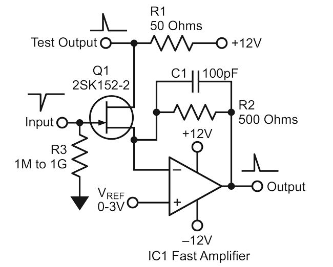
Various JFETs have been tested for this Design Idea circuit (Figure 2): Sony 2SK152-2, Interfet IFN152, and Siliconix/Vishay/OnSemi J309, as they have high gain and a low gate leakage current of about 100 pA. These JFETs are well suited to 1MΩ- to 1GΩ-input impedance amplifier design. The circuit works well to over 100 MHz.
 |
|
| Figure 2. | Very wide temperature range, gain-stable, fast JFET high-impedance amplifier. |
One advantage of the circuit comes from its large operating temperature range (–55 °C to 125 °C for the JFET). IC1 can be kept at room temperature, linked by a few feet of PTFE coax for example, for temperature isolation. Thus the JFET can be mounted in a very cool environment for lowest noise, which was a primary objective of the design.
The input signal to JFET Q1 is fed to its gate, which is biased to ground through R3 (which could be a lower value in the case of a current-source input).
The JFET’s source is biased through the inverting current-to-voltage stage based on IC1. VREF, which controls the quiescent VGS, is set between 0 V & 3 V for most JFETs to set the drain current at the zero-drift midpoint, which also gives a large dynamic range for the input signal. By adjusting VREF, we can bring Q1’s operating current to about 7 mA-10 mA, which is close to the zero-drift point. The operating current has to be separately analyzed for each JFET to be set properly. For the 2SK152-2, it was found to be 7.5 mA ±1 mA for the 1,000 JFETs I have tested.
IC1 is a fast CFA (current-feedback amplifier): Analog Devices’ AD812 at ±12 V to ±15 V, and AD8009 at ±5 V, have been used successfully. The feedback resistor R2 can be from 500 Ω to 5 kΩ, in parallel with C1 of 100 pF to avoid oscillations and overshoot. Remember that the output of the amplifier has a voltage offset due to the biased input stage and hence is best suited to AC or pulsed signals. A risetime of 10 ns to 100 ns is feasible with the proper R2/C1 combination. CFAs are operated within a gain range of 2-10, set by resistor R2; at much higher gains, the amplifier starts oscillating.
R1 provides a test output to measure the current through the JFET. It also generates a fast 50 Ω output which can be directly connected to an oscilloscope. Both output signals are inverted compared to the input signal – typically ±100 mV. For DC-biased signals, a coupling capacitor of about 1 nF-10 nF can be used in front of the gate.
Materials on the topic