A typical driver for thermoelectric (TE) cooler applications may use pulse width modulation (PWM) to drive an H-bridge circuit. This scheme works but drives the TE device with very large current pulses. These square waves, which are often the devices’ maximum rated current, can create substantial amounts of noise on a PCB’s power and ground planes/buses that may disturb sensitive analog circuits. It’s possible to use noise filters and PCB layout techniques to reduce the PWM-induced noise, but these measures can complicate a design, and may still not provide sufficient noise reduction for sensitive circuits.
One solution would be use a linear circuit to drive the TE cooler, thereby eliminating the PWM driver’s high dv/dt, high-current pulses. On the other hand, linear drivers tend to be inefficient, resulting in much more heat dissipation in the driving devices.
This Design Idea’s circuit employs a third approach, based on an H-bridge driver topology. In this circuit, the pass transistors run at close to their saturation points to reduce dissipation losses. After familiarizing you with the circuit, we will compare 5 V and 3.3 V power voltage cases.
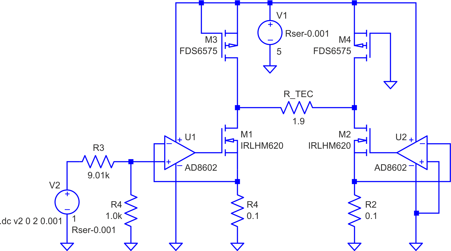
Using voltage-controlled current sinks on the low side of the bridge, operated near saturation at full scale, and fully-saturated switches on the high side allows us to reduce the power-supply voltage to the point where the sum of the voltage drops in the pass transistors and the load is just less than the supply voltage required to produce the driver’s maximum output current (Figure 1).
 |
||
| Figure 1. | The H-bridge is driven by analog signals for the VCCS in the low side and digital signals to switch the current polarity, which reverses the heat flow. |
|
Using this architecture, the power supply voltage can be adjusted to minimize wasted power, while allowing close to full rated current to flow in the TE cooler on demand. Selecting very low RDS(ON) FETs and current sense resistors at close to the minimum practical value can help to reduce the wasted power. For this application, the FET’s VTH specification must be less than 2 V.
 |
||
| Figure 2. | When the power voltage is 5 V, the maximum power dissipation of driver transistor M1 is 3.15 W at I(TEC) = 1.25 A. At full range current, 2.0 A, M1’s dissipation is 1.9 W. |
|
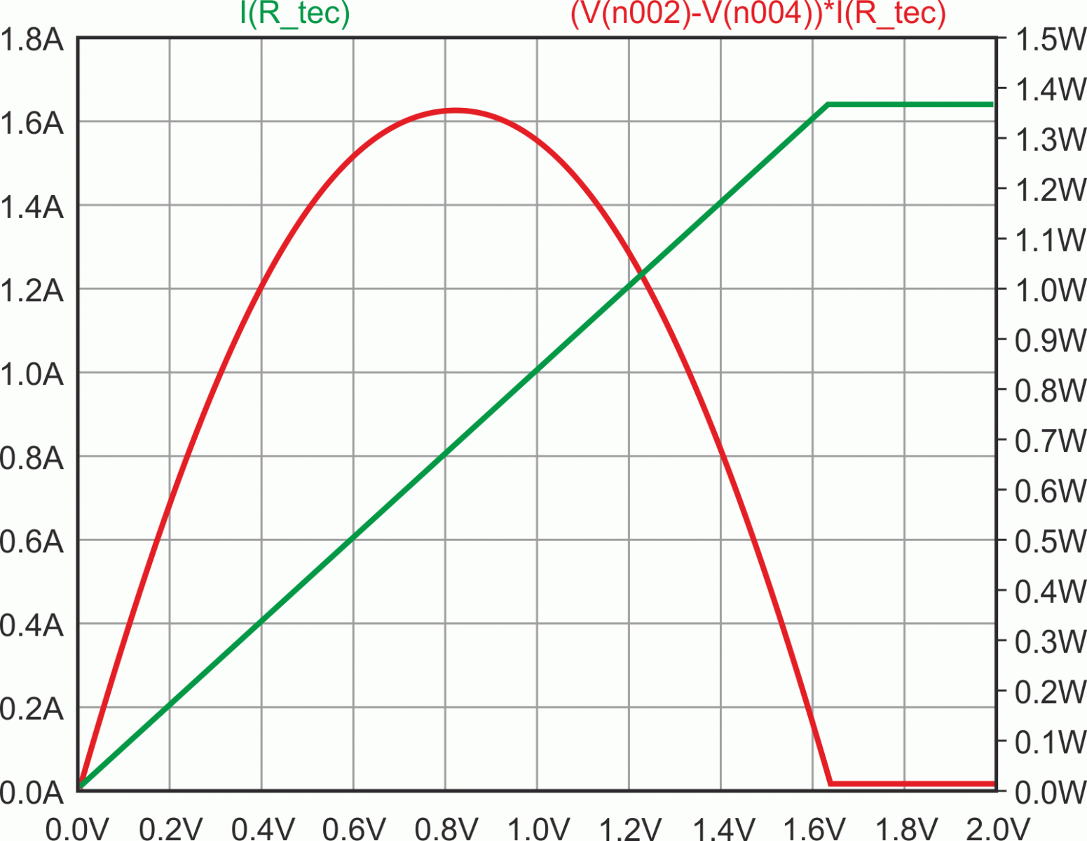
By reducing the supply voltage from 5 V to 3.3 V, full scale current has been reduced from 2 A at 2 V input, to 1.63 A at 1.63 V input (Figures 2 and 3). As long as this does not impact the heat flow requirements of the design, the benefits are clear; peak dissipation in the current pass transistors has been reduced from 3.3 W to 0.8 W, a 75% reduction in heat loss.
 |
||
| Figure 3. | Reducing the power source to 3.3V reduces driver transistor M1’s peak dissipation to 1.35 W at I(TEC) = 0.8 A. At full range current, 1.65 A, M1’s dissipation is just 20 mW. |
|
The dissipation in driver transistor M1 at 1.63 A (comparing equal load currents for the 5 V and 3.3 V supply cases) has been reduced from 2 W to ~20 mW (Figure 3).
The maximum dissipation in driver transistors M3 and M4 occurs at full scale current. These devices are operated in saturation or cutoff, so the dissipation never exceeds a few tens of milliwatts.
The efficiency afforded by this linear driver solution is especially suitable for battery-powered TE cooler applications. The circuit also provides advantages in AC line-powered systems, by eliminating the electrical noise created by sharp-edged PWM current pulses.
The example circuit in Figure 1 shows only cooling (or heating, depending on how the TE cooler is installed) drive for simplicity, but it can be easily adapted for bi-modal operation. For applications where digital control is needed, it is fairly simple to connect the cooler drive circuits to a microcontroller’s digital and analog outputs to achieve both heating and cooling operation.