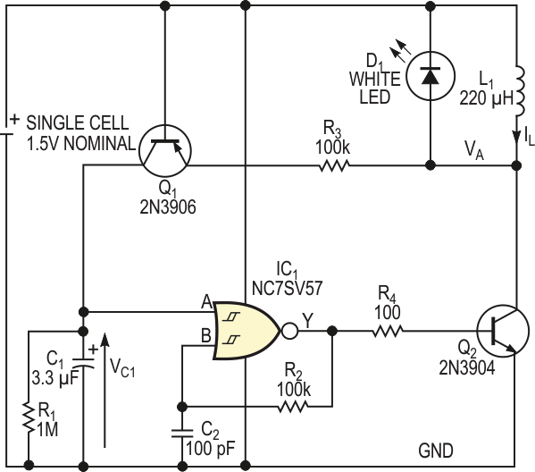
The white-LED flasher in Figure 1 offers an alternative approach to a previously published idea (Reference 1). Targeting use in portable appliances and products powered by a single cell, this circuit flashes an LED to provide a highly visible warning signal – for example, to indicate power on, battery low, or another eye-catching visual signal. However, white LEDs typically present a forward-voltage drop of 3 to 5 V. Given that a single cell's end-of-life output voltage decreases to 1 V, flashing a white LED from such a low voltage demands special circuit techniques. The circuit in Figure 1 exploits the low-voltage capabilities of Fairchild's universally configurable two-input NC7SV57 logic gate. The NC7SV57 operates from a supply voltage as low as 0.9 V, a key requirement for single-cell applications.
 |
|
| Figure 1. | A few inexpensive components can light a white LED from a single primary cell. |
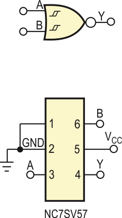
Available in a six-lead SC70 package, this IC features Schmitt-trigger inputs. You can configure the device to implement AND, NAND, NOR, Exclusive-NOR, and invert logic functions. Connecting the pins as in Figure 2 produces a two-input NOR gate. Upon initial power application, capacitor C1 is uncharged, and its voltage, VC1, is 0 V. With C1 holding Input A low, IC1 temporarily becomes an inverter and forms a simple astable relaxation oscillator at a frequency that C2 and R2 determine. The square-wave signal at IC1's output drives switching transistor Q2.
 |
|
| Figure 2. | Connecting pins 1 and 2 to ground configures the NC7SV57 as a two-input NOR gate. |
When IC1's output pulses high, Q2 turns on and saturates, sinking current, IL, through inductor L1. The inductor current ramps up at a rate determined mainly by VBATT; L1's inductance; and Q2's on-time, tON. During this interval, LED D1 and Q1's base-emitter junction are reverse-biased. Provided that the inductor does not saturate, current IL ramps up linearly and reaches a peak value, IL(PEAK) at the end of the on-time.
When IC1's output goes low and Q2 turns off, L1 generates back EMF to forward-bias D1 and raises its anode voltage, VA, to a value greater than VBATT. Current circulates through L1 and D1 and ramps down to zero as L1's stored energy decays. Values of 100 pF for C2 and 220 kΩ for R2 set the astable oscillator's frequency at approximately 20 to 30 kHz. On each cycle, a current pulse with a peak value, IL(PEAK), flows through the LED. Due to the high repetition frequency and persistence of vision, the LED appears to be continually on.
Without Q1 and R3, the astable circuit would oscillate without interruption and continuously illuminate the LED. However, Q1 and R3 provide a charging path for C1. On any cycle of the astable square wave during which VA rises above VBATT, Q1's base-emitter junction becomes forward-biased via R3, allowing a pulse of current to flow through Q1 into C1. The magnitude of this current pulse depends largely on D1's forward-voltage drop and R3's resistance. Each current pulse applied to C1 slightly increases the capacitor's charged voltage. When the charged voltage eventually exceeds IC1's upper input- threshold voltage, VTU, at Input A, the astable oscillator shuts off, and IC1's output goes low. In response, Q2 and the LED turn off, and current pulses cease to flow through Q1.
Next, C1 discharges through R1, and VC1 decays at a rate that only the R1-C1 time constant determines. D1 remains off until VC1 falls below the Schmitt trigger's lower threshold voltage, VTL; astable oscillations recommence; and the LED again turns on and repeats the illumination cycle.
For the values of C1 and R1 in Figure 1, the LED's on-time is roughly proportional to R3's resistance. A relatively small value produces a short "blink," whereas a higher resistance leads to an on-time of several seconds. The LED's off-time depends only on the values of C1 and R1. To ensure that VC1 can exceed IC1's upper input-threshold voltage, R1's resistance must exceed R3's resistance.
You can use a small-signal pnp transistor with good current gain for Q1, because its specifications aren't critical. However, to ensure that most of the battery voltage appears across L1 when Q2 conducts, use a switching transistor with low collector-emitter saturation voltage for Q2. If the saturation voltage is low enough to neglect, you can calculate the peak current in L1 using VBATT×tON/L1. The LED's intensity is proportional to its average forward current and thus determined in part by IL(PEAK). For optimum LED brightness, select the on-time and L1 to maximize IL(PEAK) but not to exceed D1's and L1's maximum current ratings. The actual value of L1 isn't critical, but values of 100 to 330 µH provide good performance and reasonable efficiency.
For large values of C1, R1, and R3, the LED flashes at a fairly slow rate. With values of 3.3 µF for C1, 1 MΩ for R1, and 100 kΩ for R3, the circuit produces a flash rate of approximately 0.4 Hz with VBATT of 1.6 V. Reducing VBATT to 0.8 V results in little flash-rate variation. At VBATT of 1.6 V, the LED delivers brightness that remains even when battery voltage decreases to 0.8 V. The circuit continues to operate when VBATT decreases to 0.65 V, although the LED dims considerably at that level.
The NC7SV57's guaranteed operating voltage ranges from 0.9 to 3.6 V, which allows operation from one or two alkaline or rechargeable nickel-cadmium cells or from a single 3 V lithium cell. Texas Instruments' SN74LVC1G57 offers the same logic functions but operates over a slightly higher supply voltage range of 1.65 to 5.5 V. To eliminate flashing operation, simply omit C1, R1, R3, and Q1. To turn the LED on or off, you can apply a gating signal to IC1's Input A.
