Switcher Adds Programmable-PWM-Duty-Cycle Clamp

Power-supply applications require the use of a duty-cycle clamp. Such applications include those using current-sense transformers and two-switch forward converters. If a duty-cycle clamp is not present, the transformers could saturate, causing a catastrophic failure in the system. However, to drive down the cost of the design, many power-supply designers use inexpensive, eight-pin PWM controllers that have no duty-cycle clamp. This Design Idea shows how to add an inexpensive duty-cycle clamp to these PWM controllers.

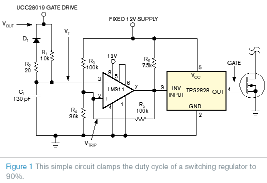
You can add the circuitry to most PWM controllers to provide a programmable duty-cycle clamp. The circuitry comprises a few passive components, a hysteretic comparator, and a gate-driver IC. Resistor R1 and capacitor C1 program the duty-cycle clamp’s dead time. Resistor R2 and diode D1 reset the timing circuitry when the output of the PWM controller goes low. Resistors R3, R4, and R5 set the comparator’s trip point, VTRIP, at 5 V. Resistor R5 adds –2.5 V of hysteresis to the comparator to ensure circuit stability.

The following example shows how to set the circuitry in Figure 1 for a maximum duty cycle, DMAX, of 0.9. The PWM controller operates at a switching frequency, fS, of 100 kHz. Most PWM controllers cannot reach 100% duty cycle and have a specified dead time. For this example, the dead time is 300 nsec. To set the timing capacitor also requires knowing the maximum output of the PWM output voltage, VOUT. In this example, the maximum output voltage is 12 V. The timing capacitor is roughly 130 pF. The design uses a standard, 120-pF capacitor. The following equations describe the calculations: t=(1–DMAX)(1/fS)–dead time=700 nsec, and

Switcher Adds Programmable-PWM-Duty-Cycle Clamp
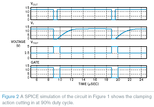
results of this simulation. VOUT is the output of the PWM controller, VT is the voltage at the inverting pin of the comparator, VTRIP is the voltage at the noninverting input of the comparator, and gate is the output of the gate-driver IC

A SPICE simulation with the circuitry in Figure 1 ran to ensure that the duty-cycle clamp works with the circuitry. Figure 2 shows the results of this simulation. VOUT is the output of the PWM controller, VT is the voltage at the inverting pin of the comparator, VTRIP is the voltage at the noninverting input of the comparator, and gate is the output of the gate-driver IC. From the waveforms in Figure 2, you can see that the duty-cycle clamp appears to be working correctly, clamping the output of the gate driver to 90 %.

EDN