Many products require an auxiliary dc output to power external devices or subsystems. If such subsystems are to be hot-connected, the auxiliary output must be protected against short circuits. Schemes using fuses are slow and will cause the internal dc-rail to drop, possibly affecting the main system.
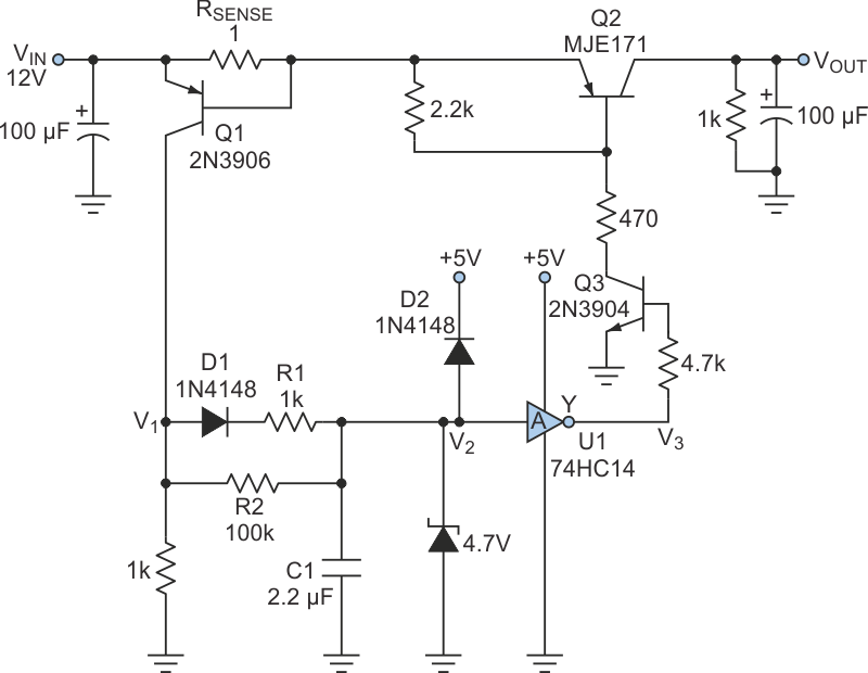
The circuit shown in the Figure 1 provides pulse current limiting at a very low cost. It can handle momentary or continuous short circuits at the output. The only effect on the input rail is a small glitch (hundreds of millivolts for hundreds of microseconds). U1 is a Schmitt trigger inverter (74HC14), Q2 is the switch, and RSENSE is the current-sense resistor. For this circuit, VIN = 12 V, and the circuit is designed for load currents up to 0.6 A.
 |
||
| Figure 1. | For less than 50 cents, this auto-resetting circuit delivers pulse current limiting. |
|
Under normal conditions – a load current under 500 mA – Q1 is off, V1 = 0 V, V2 = 0 V, C1 is discharged, and V3 = 5 V. Q3 is on, Q2 is on, and VOUT = 12 V.
If the load current goes above 0.6 A, Q1 turns on, V1 increases, and C1 charges through D1 with a small time constant (C1 × R1). When V2 increases above the upper trip point of 74HC14, V3 goes low and Q3 turns off, Q2 is switched off, and the load current goes to zero. Then Q1 switches off, V1 goes low, and C1 discharges with a large time constant (C1 × R2). After a longer duration (depending on C1 and R2), V2 goes low, V3 switches high, and the series switching transistor (Q2) turns on.
If the short circuit is continuous, this pulsed switching continues, on and off. For high-current applications, power dissipation in RSENSE becomes a problem. Therefore, Q1 can be substituted with a high-side current sensor that has amplification (like a Zetex ZXCT1021), with suitable circuit modification. D2 is a protection diode for discharging C1 when the power is switched off. Q2 should have a sufficient current rating (preferably 4 to 5 A). Designers should also consider Schmitt-trigger trip point tolerances. Q2 can also be substituted with a P-channel MOSFET for a lower forward drop. For higher voltages (e.g., 24 V), the MOSFET gate source should be protected: It must not exceed the breakdown voltage of a Zener diode.
When the output was shorted with a 1-Ω resistor, the resulting V2 was a sawtooth waveform between 2 and 3.2 V, with a rise time of 500 μs and a decay time of 1 s. The amplitude of the output current pulse was approximately 1.5 A for 500 μs, and the glitch at the input rail was 0.2 V for 500 μs. C1 can be a lower value (say, 0.47 μF) to reduce the short-circuit current pulse width.
