Eric Schlaepfer, Maxim Integrated Products
EDN
Microprocessors, microcontrollers, and SOCs (systems on chips) often need a reset pulse to initialize properly. Many of these devices also use separate I/O- and core-voltage supplies. When you use multiple supplies, you must turn them on in a specific sequence to prevent the circuits from ending up in an unknown state or burning out due to unexpected current paths. You should also monitor the voltages to ensure that the device does not come out of reset until both voltages settle to levels within the operating-voltage range.
A previous Design Idea presents a circuit performing the reset function (Reference 1). Unfortunately, this circuit suffers from a number of limitations. For example, it does not monitor the voltage on the 3.3 V rail. The 3.3 V rail acts as a reference, so the 1.8 V rail suffers from poor monitoring accuracy. Further, the reset delay may not be present if you sequence the power rails in the reverse order, and the reset pulse has a glitch that could cause problems with the SOC. Finally, the reset-delay capacitor may reset incorrectly if you rapidly cycle power.
 |
||
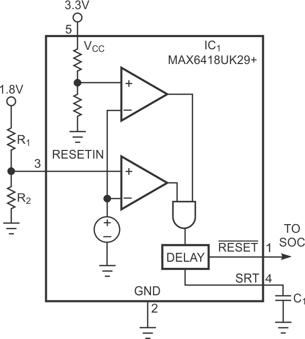
| Figure 1. | This circuit provides a microprocessor or an SOC with a clean reset pulse. |
|
The circuit in Figure 1 uses a reset IC to provide a glitch-free reset pulse with a well-defined pulse width. It accurately monitors both the 3.3 and the 1.8 V rails. You adjust resistors R1 and R2 to set the monitoring threshold for different core voltages using the equation
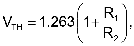
where VTH is the threshold voltage. You adjust C1 for different pulse widths. You calculate C1 using the following formula:
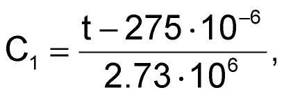
where t is the desired delay in seconds and C1 is in farads.
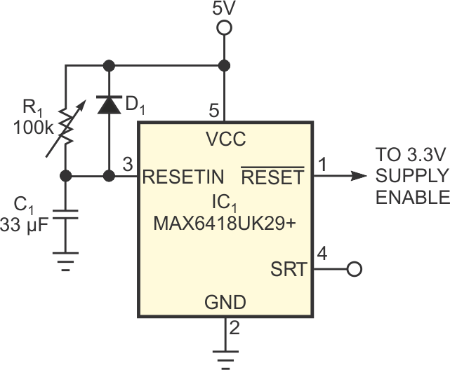
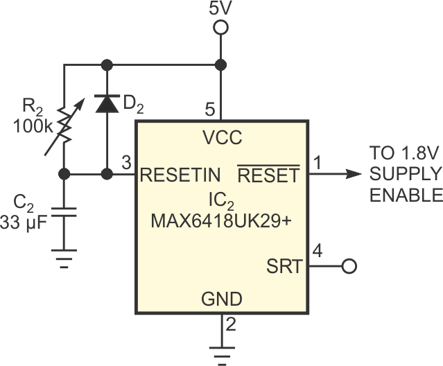
Two other previous Design Ideas present circuits for sequencing the two power-supply rails (references 2 and 3). One circuit requires many components to achieve a simple function, and the other circuit requires a microcontroller-firmware-development tool set. A simpler alternative implements a sequencing circuit using two ICs acting as voltage detectors (Figure 2). This circuit is useful when performing experiments to determine the proper sequencing order. You adjust R1 and R2 to set the sequence delay for each power rail. Each IC monitors the voltage on the RC circuit and asserts its output when the capacitor voltage crosses the threshold.
|
||||||
| Figure 2. | Sequence two power supplies using R1 and C1 to set the delay. | |||||
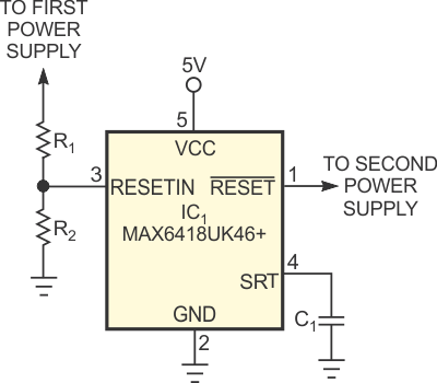
Once you determine a sequence order, you can implement the power sequencing with a single IC (Figure 3). This approach monitors the output voltage of the previously sequenced power supply before enabling the next power supply. It also monitors the 5 V rail.
 |
||
| Figure 3. | C1 sets a delay to sequence two power supplies. | |
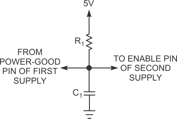
For cost-sensitive applications, you can devise a passive circuit (Figure 4). It works, although the sequence delay is not well-controlled and the voltages are not monitored. In this case, the open-drain output from the first supply holds the node low until power is good. When the open-drain output releases the node, C1 charges through R1, asserting the active-high enable of the second supply. You choose R1 and C1 to determine the sequence delay.
 |
||
| Figure 4. | Use this circuit to try different sequencing delays and adjust the sequencing order. |
|
