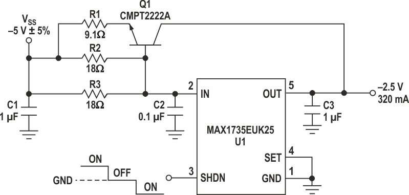
Adding four components to a negative linear regulator (U1 in the Figure 1) increases the load current by 60%. The additional pass transistor and associated resistors cost less than $0.17 in 1000-unit quantities.
 |
||
| Figure 1. | A pass transistor and associated resistors boosts load current in this negative linear regulator by 60%. | |
Connecting the SET terminal to ground keys U1's output voltage to –2.5 V. U1's maximum load current is 200 mA. The extra components (Q1, R1, R2, and R3) draw another 120 mA maximum from the load. This produces a total maximum load current of 320 mA without degrading the output regulation.
In addition to reducing the power dissipated in Q1, R1 prevents thermal runaway in Q1 and provides momentary protection against a short-circuited output. By limiting gain in the Q1 loop, R1 also prevents oscillation. Current flowing through U1 from OUT to VSS produces a voltage drop of VR2 across R2 and R3, which enables Q1 to conduct load current as VR2 approaches the base-to-emitter threshold of Q1. This threshold (VBE) is approximately 0.7 V at room temperature.
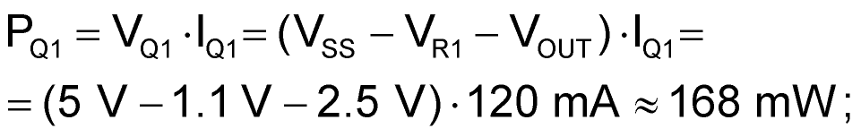
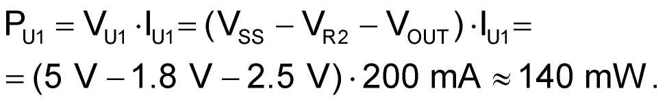
Choose the values of R1, R2, and R3 to ensure that R2, R3, and Q1 dissipate maximum power at the maximum load current (320 mA in this case). At 320 mA, U1 conducts 200 mA and Q1 conducts 120 mA. Component power dissipation at maximum load is as follows:


To provide higher load current, you can easily modify the circuit by increasing the power-dissipation ratings of R1, R2, R3, and Q1. The Table 1 details the components shown for a 320-mA load current. For power dissipation, the circuit board should have ample copper connected to the leads of power-dissipating components. Heat then conducts through the component leads to the circuit board, spreads into the copper areas, and exits the board through convection.
| Table 1. | Components used in example circuit | |||||||||||||||||||||||||
|
||||||||||||||||||||||||||