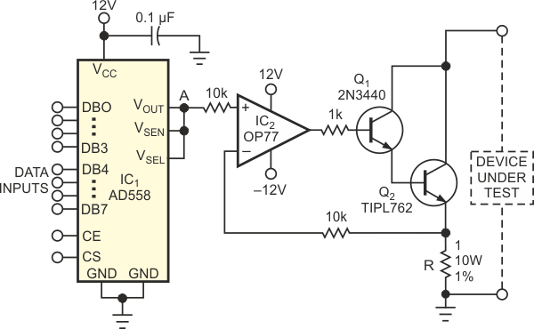
The circuit in Figure 1 serves as a variable, current-sink load for testing voltage sources. You use digital commands to set the load current of the device under test over a wide range, independently of the device under test's output voltage. The circuit comprises an AD558 DAC, IC1, which provides a reference voltage at Point A. Practically any type of DAC converter works well in this application. The AD558 is a single-supply type with an internal reference; these features simplify the design. IC1 generates an output voltage of 0 to 2.55 V (Table 1). The control inputs CE and CS in IC1 allow you to control the DAC from a microprocessor bus. If your application does not involve a data bus, connect CE and CS to ground to obtain direct access to the DAC's data inputs.
| Table 1. |
DAC output voltage versus input code |
| Digital input of IC1 |
Voltage at Point A (V) |
| Binary |
Hexadecimal |
| 0000 0000 |
00 |
0 |
| 0000 0001 |
01 |
0.01 |
| 0000 1111 |
0F |
0.15 |
| 0001 0000 |
10 |
0.16 |
| 1000 0000 |
80 |
1.28 |
| 1111 1111 |
FF |
2.55 |
|
| |
 |
| Figure 1. |
A simple circuit allows digital control of current, independent of voltage. |
The second part of the circuit in Figure 1 consists of an op amp, IC2, driving transistors Q1 and Q2. IC2 compares the reference voltage at Point A with the voltage across resistor R. IC2’s output voltage controls Q1 and Q2 such that the voltage across R equals the reference voltage at point A. The voltage across R is proportional to the current from the device under test and is independent of the output voltage of the device under test. The value of R in Figure 1 is 1 Ω; thus, the circuit provides a sink current of 1 A when the voltage at point A is 1 V. With the values shown in Figure 1, you can control currents of 0 to 2.55 A over a device under test voltage range of 5 to 250 V. Be sure to limit the power dissipation in Q2 to 120 W.
Materials on the topic
- Datasheet Analog Devices AD558
- Datasheet Analog Devices OP77
- Datasheet STMicroelectronics 2N3440
- Datasheet Bourns TIPL762
