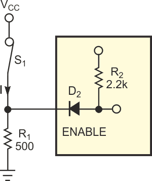
The control circuit in Figure 1 presents a relatively low input resistance and thus imposes a low value on external pulldown resistor R1 to provide the desired low-level input voltage. In turn, R1 wastes power by drawing a relatively high current through switch S1. For example, suppose that the control circuit presents an input resistance of 2.2 kΩ and requires a logic-low input of 5 V or less. At a VCC of 24 V, R1 must not exceed 500 Ω for a current drain of 24/500 = 48 mA. The power dissipated in R1 is thus 242/0.5 = 1152 mW, which requires a 2 W resistor for reliable operation.
 |
|
| Figure 1. | A conventional network requires a low-value pulldown resistor. |
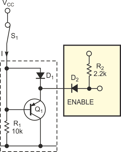
In this application, the system includes three controls with three input circuits, which present a total current of 432 mA and adds approximately 10 W to the power budget. To reduce wasted power, it uses an active pulldown circuit (inside the dashed line in Figure 2). As long as switch S1 remains closed, PNP transistor Q1’s base voltage exceeds its emitter voltage due to diode D1’s forward voltage drop. Thus, Q1 doesn't conduct, and the control circuit's input voltage rests at VCC – 0.7 V (D1’s forward voltage drop).
 |
|
| Figure 2. | An active pulldown circuit substitutes a saturated transistor for a power-consuming pulldown resistor. |
Opening S1 reverse-biases D1, and the base current flowing through resistor R1 turns on Q1, which saturates and pulls the circuit's input to VCE(SAT). Closed-circuit current through S1 is thus VCC/R1. For example, with VCC of 24 V and R1 having a value of 10 kΩ, I = 24/10 = 2.4 mA, and R1 dissipates 0.058 W, or approximately 20 times less power than in Figure 1. In this application, current demand of the nine control-circuit inputs decreases from 432 to 22 mA and saves pc-board space by eliminating the need for using 2 W.
 |
|
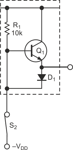
| Figure 3. | Rearranging the circuit and using an NPN transistor for Q1 yields an active-pullup network. |
As a variant, Figure 3 shows an active-pullup version of the circuit.