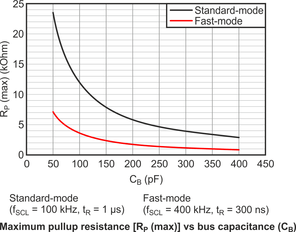
The popular I2C communication standard manages to perform flexible serial I/O with just a super simple two pin bus: SCL and SDA. It accomplishes this trick with bidirectional timing and data flow. Bidirectional flow is good at saving pins but due to its use of passive pullup resistors, not so good at saving power. Bus pullup resistances must be chosen low enough (and therefore pass sufficient current) to charge parasitic bus capacitance at the speed dictated by the chosen data rate. Figure 1 illustrates this inconvenient arithmetic.
 |
|
| Figure 1. | I2C bus speed inversely affects maximum effective pullup resistance. Source: (Ref. 1). |
The amount of V/R current drawn and V2/R power squandered in passive “pull-upping” depends on bus capacitance, pullup voltage, and duty cycle; and as Figure 1 shows, for fast-mode 400 kHz, V = 5 V, and CB = 400 pF can be as much as 5 V/1k = 5 mA and 52/1k = 25 mW. This can easily comprise a sizable fraction of total system power use. This is bad for batteries and bad for political correctness in the age of “greenness” and “sustainability”.
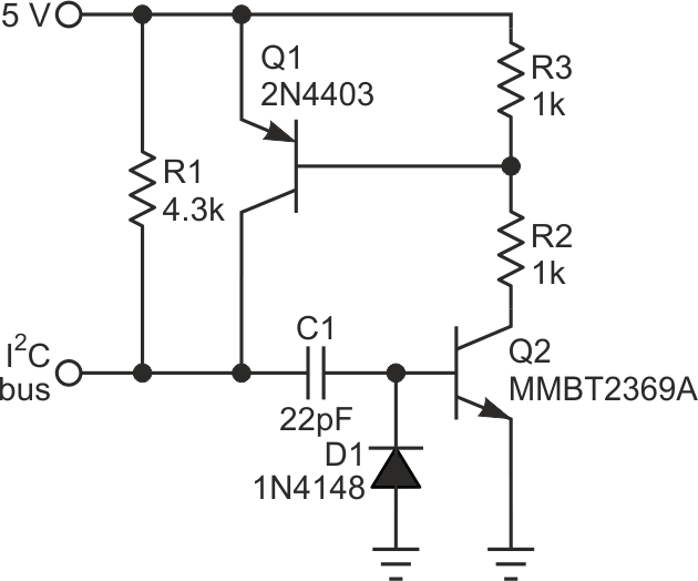
So how to save some of that excess current and power? Figure 2 shows one way: an active pullup with values chosen for the worst-case combination illustrated in Figure 1 of high speed (400 kHz) and high capacitance (400 pF).
 |
|
| Figure 2. | Regenerative active pullup circuit (one of two needed) with values chosen for the worst-case combination shown in Figure 1. |
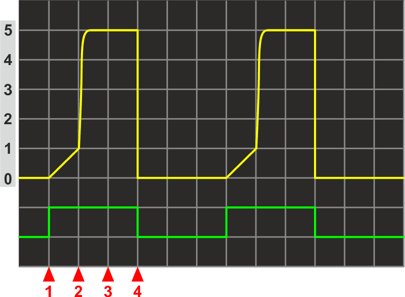
This simple circuit topology, given that saving pullup power was its avowed purpose, begins on an unpromising note: a passive pullup resistor R1. How the whole thing works is diagrammed in Figure 3.
 |
|
| Figure 3. | Active pullup waveforms and 4-step sequence labeled within the image. |
The active pullup process occurs in four steps.
- Release of the bus signal line in question (i.e., SCL or SDA) allows R1 to begin passive pullup and start charging bus capacitance. The resulting voltage ramp is slow because R1 is more than 4x larger than the 1k calculated as necessary in Figure 1. It’s obviously never going to complete risetime soon enough!
- But wait: The resulting signal is being coupled by C1 to Q2’s base. Consequently, at Step 2 of the process, Q2 turns on, taking Q1 with it and initiating a very fast positive feedback loop that drives both transistors into saturation and completes bus capacitance charging in order of tens of nanoseconds; removing the voltage drop across R1 and ending its power drain.
- The very short time constant of 22 pF C1 working into Q2’s base impedance discharges C1 and terminates drive for the transistors, allowing them to begin turn off and end active pullup. This gives Q1 and Q2 time to recover from saturation.
- Pulldown begins the next cycle of bus activity and recharges C1 through D1, which also protects Q2’s limited (only 4.5 V) maximum reverse VBE rating.
Thus, our parable of parsimonious pullup power is given a happy ending, with about a 75% saving of the power otherwise required, and without any need for software modification.
