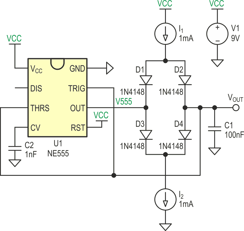
The circuit works due to the fact that voltage increases or decreases linearly when a constant current flows into or out of a capacitor. If we manage to charge and discharge the capacitor with the same constant current, then the voltage of the capacitor will become a triangular wave; that’s the crux of this circuit (Figure 1).
 |
|
| Figure 1. | Circuit schematic of triangle/sawtooth wave generator using 555 timer. |
Assuming that the circuit has reached steady-state, then the working principle is as follows: When the voltage across capacitor is 1/3VCC, the 555’s output will be high, making D1 and D4 reverse biased but D2 and D3 forward biased. Therefore the capacitor will charge through D2 with a constant current I1 (its voltage will increase linearly) until its voltage reaches 2/3VCC. When that happens, the 555’s output will be low, making D3 and D2 reverse biased but D4 and D1 forward biased, thus discharging the capacitor through D4 with a constant current I2. If I1 is equal to I2, then it takes the same amount of time to go from 1/3Vcc to 2/3VCC and vice versa. However, if I1 is different from I2, we can generate different waveforms such as positive and negative sawtooth waves.
 |
|
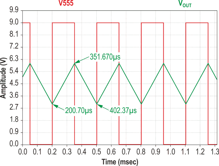
| Figure 2. | Simulation of triangle/sawtooth wave generator circuit shown in Figure 1. |
The expression for the rise time (TRISE) and fall time (TFALL) is the following:
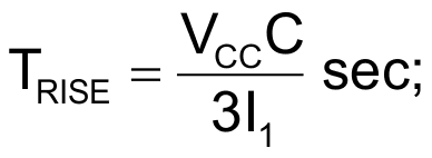
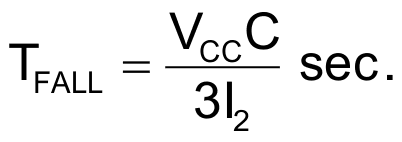
If we make I1 and I2 dependent on VCC, we can eliminate the dependency on VCC, this makes the above expressions only depend on fixed parameters (more on that later).
For simulation purposes let’s assume that C = 100 nF, I1 = I2 = 2 mA and VCC = 9 V, therefore TRISE = TFALL = 150 µs. As shown in Figure 2, the circuit works properly.
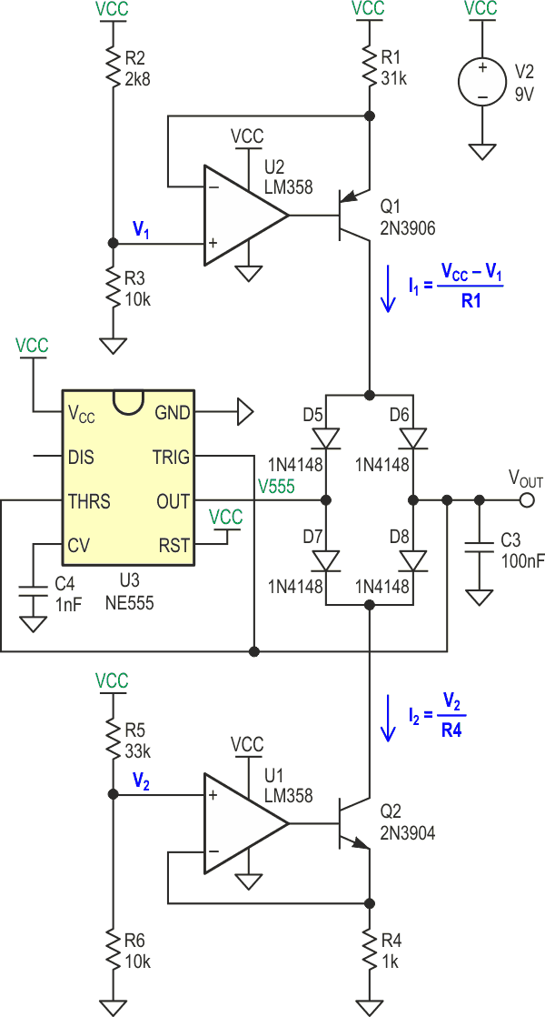
Let’s now move to the real circuit and look at some real waveforms. The basic principle is the same but I1 and I2 are replaced by current sources created with one LM358 and two transistors (Q1 and Q2) (Figure 3).
 |
|
| Figure 3. | Schematic of triangle/sawtooth wave generator with an LM358 and two transistors used as current sources. |
Now we have to take into consideration that Q1 and Q2 never enter saturation. The maximum collector voltage of Q1 will be around 2/3VCC + 0.7 V since VCC = 9 V. Therefore, we have to design the circuit so that the emitter voltage is higher than or equal to 2/3VCC + 1 V to avoid saturation. This same principle is applied to Q2. (However, now it is the minimum voltage on Q2’s collector which is around 1/3VCC – 0.7 V, so we have to design an emitter voltage less than or equal to 1/3VCC – 1 V.) Thanks to the negative feedback of the op-amp, it is easy to do with a voltage divider (removing the dependency on VCC in equations 1 and 2) since the non-inverting and the inverting input are at the same voltage.
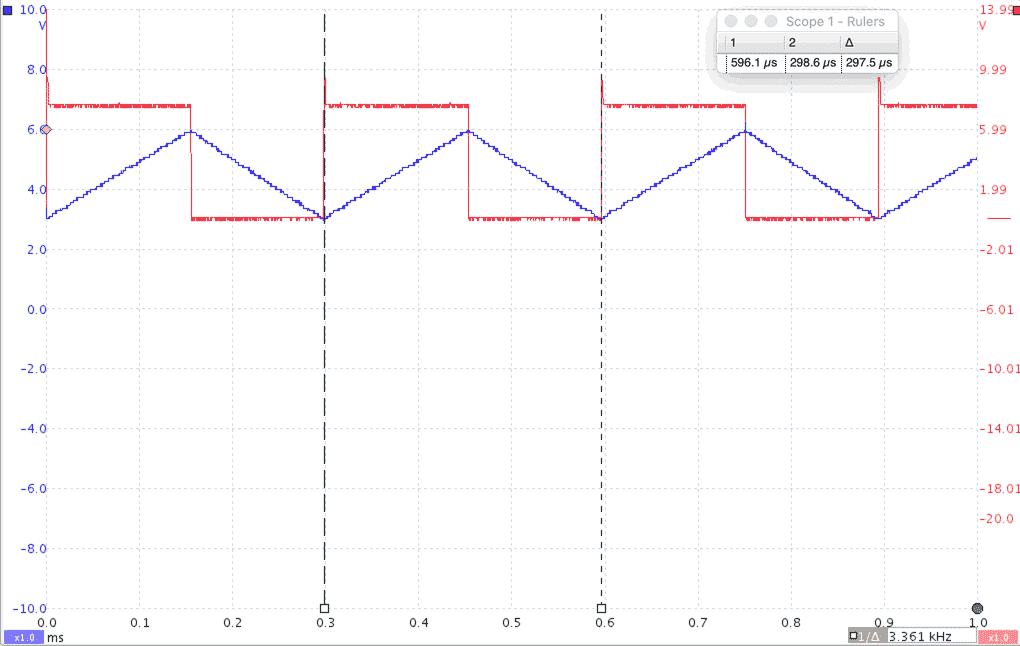
In this particular case, I1 = I2 = 2 mA, so we should have TRISE = TFALL = 150 µs. Let’s take a look at the triangular waveform (Figure 4).
 |
|
| Figure 4. | Scope capture of triangular waveforms from the circuit shown in Figure 3. |
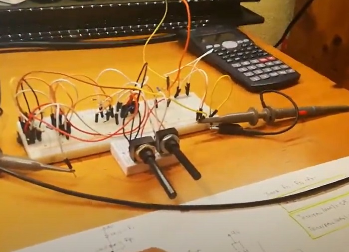
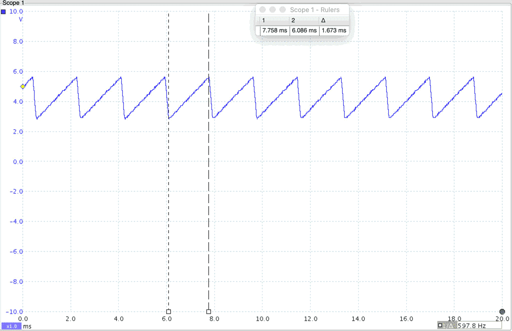
So the circuit works properly, but if I add it in series with R1 and R4 – two 10 kΩ potentiometers – we can change the total resistances at the emitters and therefore change the current I1 and I2. If, for example, we move the potentiometer of Q2 to approximately 0 Ω and the potentiometer of Q1 to 10 kΩ, then I2 = 2/1 kΩ = 2 mA and I1 = 2/11 kΩ = 181 µA, therefore it will take longer (11 times longer, around 1.65 ms) to charge the capacitor so we have generated a positive sawtooth wave (Figure 5):
 |
|
| Figure 5. | Positive sawtooth wave generated from circuit shown in Figure 3. |
Playing with the potentiometers allows you to generate an arbitrary waveform (within limits). Of course, lowering R4 or R1 will cause the I1 and I2 currents to increase and reduce the minimum falling or rising time.
