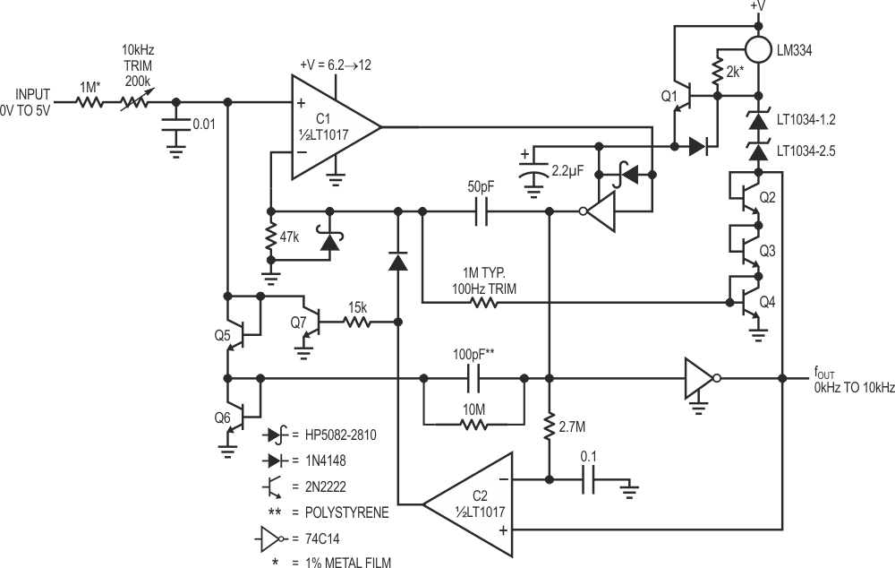
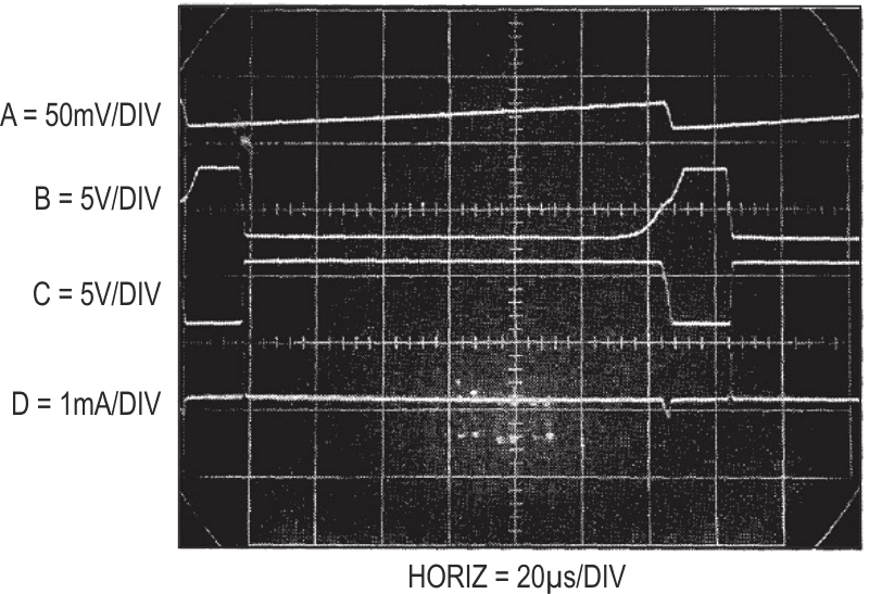
Figure 1 is a micropower voltage-to-frequency converter. A 0 V to 5 V input produces a 0 kHz to 10 kHz output with a linearity of 0.05%. Gain drift is 80 ppm/°C. Maximum current consumption is only 90 µA, almost 30 times lower than currently available V-F converters. To understand circuit operation, assume C1’s positive input is slightly below its negative input (C2’s output is low). The input voltage causes a positive going ramp at C1’s positive input (trace A, Figure 2). C1’s output is low, biasing the CMOS inverter output high. This allows current to flow from Q1’s emitter, through the inverter supply pin to the 100 pF capacitor. The 2.2 µF capacitor provides high frequency bypass, maintaining low impedance at Q1’s emitter. Diode connected Q6 provides a path to ground. The 100 pF unit charges to a voltage that is a function of Q1’s emitter potential and Q6’s drop. When the ramp at C1’s positive input goes high enough, C1’s output goes high (trace B) and the inverter switches low (trace C). The Schottky clamp prevents CMOS inverter input overdrive. This action pulls current from C1’s positive input capacitor via the Q5-100 pF route (trace D). This current removal resets C1’s positive input ramp to a potential slightly below ground, forcing C1’s output to go low. The 50 pF capacitor furnishes AC positive feedback, ensuring that C1’s output remains positive long enough for a complete discharge of the 100 pF capacitor. The Schottky diode prevents C1’s input from being driven outside its negative common mode limit. When the 50 pF unit’s feedback decays, C1 again switches low and the entire cycle repeats. The oscillation frequency depends directly on the input voltage derived current.
 |
|
| Figure 1. | V-to-F converter achieves 0.05% linearity while requiring only 90 µa supply current. |
Q1’s emitter voltage must be carefully controlled to get low drive. Q3 and Q4 temperature compensate Q5 and Q6 while Q2 compensates Q1’s VBE The two LT1034s are the actual voltage reference and the LM334 current source provides 35 µA bias to the stack. The current drive provides excellent supply immunity (better than 40 ppm/V) and also aids circuit temperature coefficient. It does this by utilizing the LM334’s 0.3%/°C temperature coefficient to slightly temperature modulate the voltage drop in the Q2-Q4 trio. This correction’s sign and magnitude directly oppose that of the –120 ppm/°C, 100 pF polystyrene capacitor, aiding overall circuit stability.
 |
|
| Figure 2. | Micropower V-to-F converter's waveforms. |
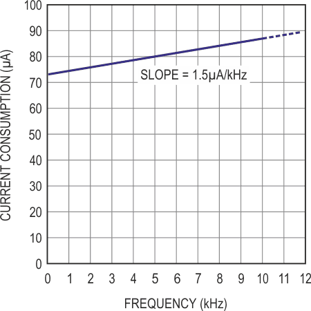
The Q1 emitter-follower efficiently delivers charge to the 100 pF capacitor. Both base and collector current end up in the capacitor. The CMOS inverter provides low loss SPDT reference switching without significant drive losses. The 100 pF capacitor draws only small transient currents during its charge and discharge cycles. The 50 pF-47k positive feedback combination draws insignificantly small switching currents. Figure 3, a plot of supply current versus operating frequency, reflects the low power design. At zero frequency, the LT1017’s quiescent current and the 35 µA reference stack bias account for all current drain. There are no other paths for loss. As frequency scales up, the charge/discharge cycle of the 100 pF capacitor introduces the 1.5 µA/kHz increase shown.
Circuit start-up or overdrive can cause the circuit’s AC-coupled feedback to latch. If this occurs, C1’s output goes high. C2, detecting this via the inverter and the 2.7M-0.1 µF lag, also goes high. This lifts C1’s negative input and grounds the positive input with Q7, initiating normal circuit action.
 |
|
| Figure 3. | Current consumption vs frequency for the V-to-F converter. |
Because the charge pump is directly coupled to C1's output, response is fast. The output settles within one cycle for a fast input step. To calibrate this circuit, apply 50 mV and select the value at C1’s input for a 100 Hz output. Then, apply 5 V and trim the input potentiometer for a 10 kHz output.