In the early days of personal computers, incorporation of one or two (or more) RS-232 serial ports as general purpose I/O adaptors was common practice. Recently, this “vintage” standard has been largely replaced (after all, it is 64 years old) by faster and more power thrifty serial interface technologies such as USB, I2C, SPI.
Nevertheless, RS-232 hardware is still widely and inexpensively available, and its bipolar signaling levels remain robustly noise and cable-length-effects resistant. Another useful feature is the bipolar supply voltages (usually ±6 V) generated by typical RS-232 adaptors. These can be conveniently tapped into via standard RS-232 output signals (e.g., RTS and TxD) and used to power attached analog and digital circuitry.
This design idea (DI) does exactly that by using asynchronous RS-232 to power and count pulses from a simple 10-kHz voltage-to-frequency converter (VFC). Getting only one bit of info from each 10-bit serial character may seem inefficient (because it is), but in this case it’s a convenient ploy to add a simple analog input that can be located remotely from the computer with less fear of noise pickup.
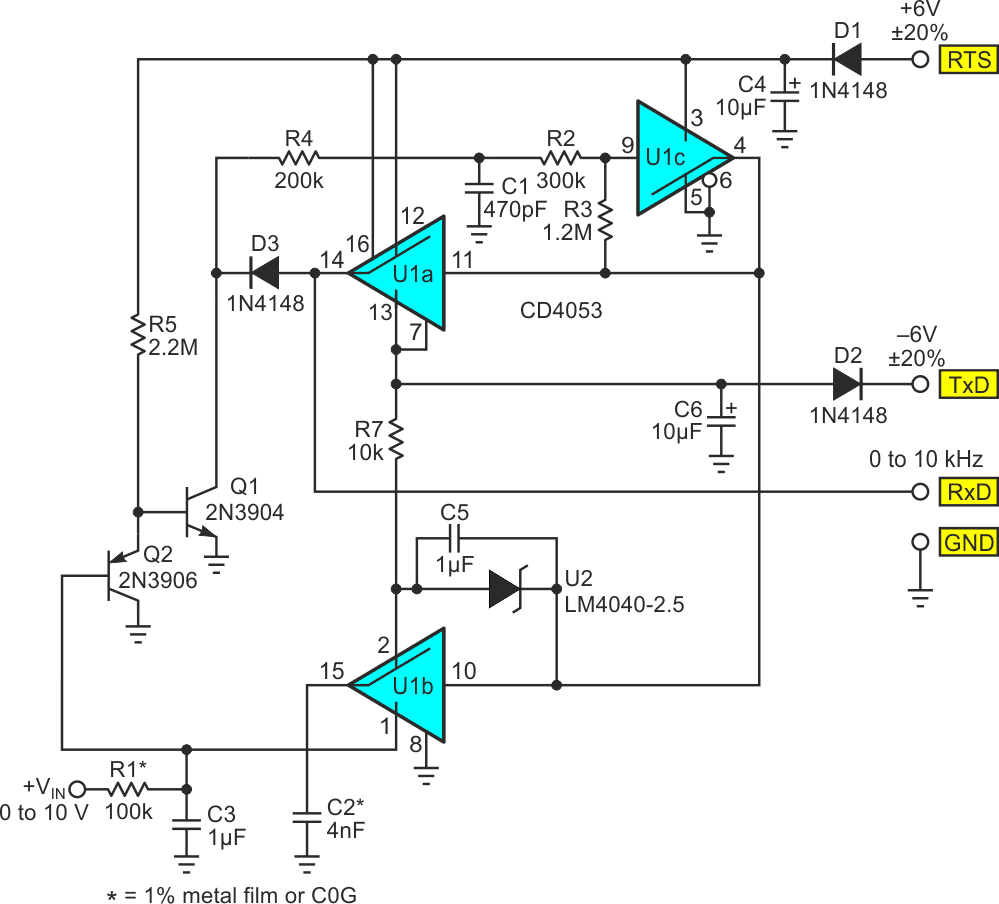
See Figure 1 for the mind meld of RS-232 with VFC.
 |
|
| Figure 1. | A 10-kHz VFC works with and is powered by a generic RS-232 port. |
Much of the core of Figure 1 was previously described in “Voltage inverter design idea transmogrifies into a 1 MHz VFC” (Reference 1).
One difference, other than the 100x lower max frequency, between that older DI and this one is the use of a metal gate CMOS device (CD4053B) for U1 instead of a silicon gate (HC4053) U1. That change is made necessary by the higher operating voltage (12 V versus 5 V) used here. Other design elements remain (roughly) similar.
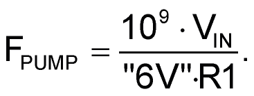
Input current = VIN/R1, charges C3 which causes transconductance amplifier Q1, Q2 to sink, increasing current from Schmidt trigger oscillator cap C1. This increases U1c oscillator frequency and the current pumped by U1a,b and C2. Because the pump current has negative polarity, it completes a feedback loop that continuously balances pump current to equal input current:


Note that R1 can be chosen to implement almost any desired VIN full-scale factor.
D3 provides the ramp reset pulse that initiates each oscillator cycle and also sets the duration of the RS-232 ST start pulse to ~10 µs as illustrated in Figure 2. Note that this combination of time constants and baud rate gives ~11% overrange headroom.
 |
|
| Figure 2. | Each VFC pulse generates a properly formatted, but empty, RS-232 character. |
The ratio of R5/R3 is chosen to balance Q2/Q1 collector currents when VIN and FPUMP equal zero, thus minimizing VIN zero offset. Consequently, linearity and zero offset errors are less than 1% of full-scale.
However, this leaves open the possibility of unacceptable scale factor error if the +6 logic power rail isn’t accurate enough, which it’s very unlikely to be. If we want a precision voltage reference that’s independent of +6 V instability, the inexpensive accurate 5 V provided by U2, C5, and R7 will fill the bill.
However, if the application involves conversion of a ratiometric signal proportional to +6 V such as provided by a resistive sensor (e.g., thermistor), then U2 and friends should be omitted, U1 pin 2 connected to –6 V, and C2 reduced to 1.6 nF. Then:

Reference
- Woodward, Stephen. "Voltage inverter design idea transmogrifies into a 1MHz VFC."