A question that arises frequently in audio and signal processing applications is this: How can I control gain on dual channel (e.g., stereo) inputs simultaneously with only a single knob? Of course, an obvious solution would be to simply use a dual element ganged pot. But ganged pots, particularly the precision multiturn variety, are relatively expensive specialty items.
 |
|
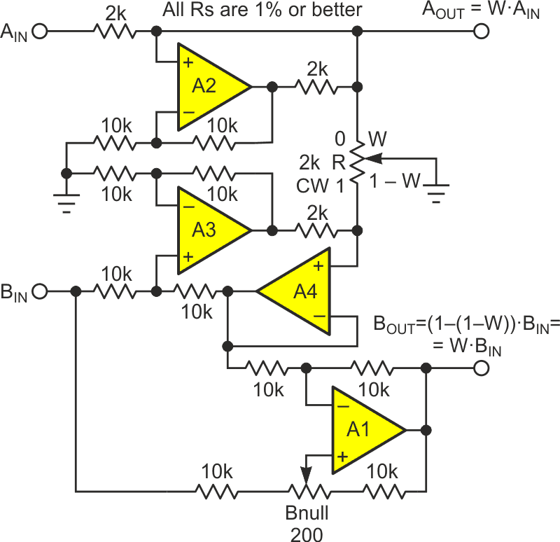
| Figure 1. | Op-amp solution requires four amplifiers comprising two Howland current pumps, a differential amplifier, and a boatload of precision resistors; it is also DC coupled. |
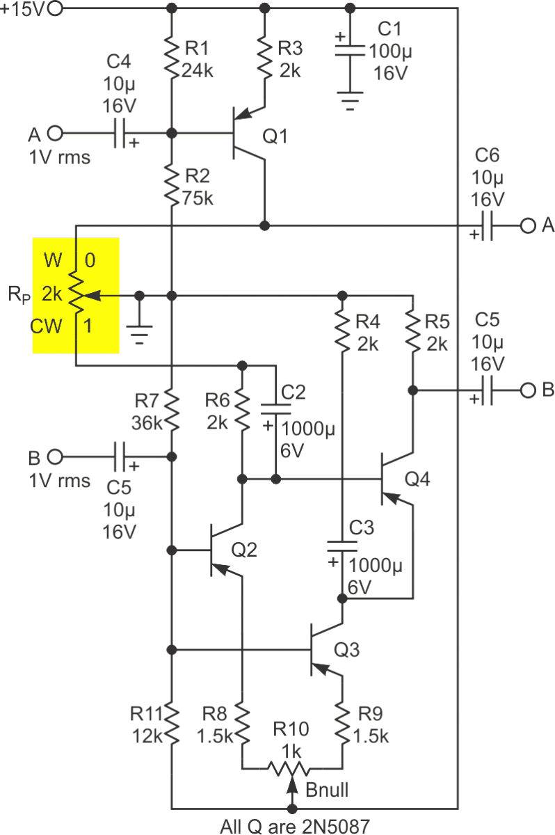
This design idea offers an alternative. It avoids the liabilities of dual element ganged pots by controlling the gain of both channels with just one ordinary single element pot, R. Two implementations are illustrated. One using a quad op-amp (see Figure 1) suitable for both AC and DC signals, and another with four discrete transistors good for AC (e.g., 20 Hz to 20 kHz audio) only (Figure 2).
 |
|
| Figure 2. | Discrete solution consists of four transistors comprising three current sources and a differencing stage and is AC coupled. |
Both schemes hinge on a connection of R with its wiper terminal grounded. This creates two mechanically linked but electrically independent variable resistances, A and B.
A = W R
and
B = (1 – W) R.
W represents R’s wiper’s position, going from 0 to 1 as R is rotated from full counterclockwise (0) to full clockwise (1). R is the total element resistance.
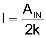
In Figure 1, amplifier A2 and its surrounding resistors are connected to create a Howland current pump, injecting

into the WR portion of the pot, to generate the AOUT signal:

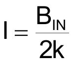
Simple enough. But what about the B channel? That starts our similarly, thanks to buffered Howland source A2 and A3, a current

is injected into the (1 – W)•R resistance to generate:

This signal is then subtracted from BIN by difference amplifier A4 to generate BOUT as:
BOUT = BIN – BIN•(1 – W) = BIN•(1 – (1 – W)) = W•BIN.
Trimmer Bnull is provided to fine tune BOUT = 0 cancellation at W = 0.
Figure 2 implements essentially the same functionality, but with AC coupling (to allow for transistor DC bias networks) and old-fashioned discrete components. I liked drawing it up mainly to prove to myself that I still remember how to work out transistor linear amplifier biasing networks!
Q1 is a straightforward current source driving the top half of the pot to generate:
AOUT = W•AIN.
Q2 does the same thing at the bottom half of the pot, generating a voltage at the base of Q4:
Q4B = B•(1 – W).
This is subtracted by Q4 from the signal generated at its emitter across R4 by Q3 to yield at the collector of Q4:
BOUT = B•(1 – (1 – W)) = W•BIN.
And look, Ma! No op-amps! Also, only one polarity power supply.
However, you may have noticed that both Figure 2’s A and B signal pathways are inverting. In audio applications this is generally not a concern so long as the inversion is symmetrical as it is here. But if it would be problematic in your intended application, you better go with the op-amp solution.