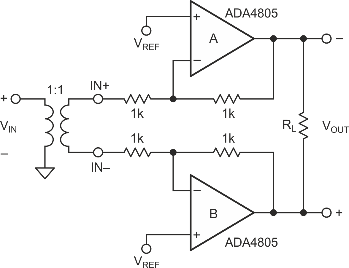
Many applications require special differential amplifiers that achieve both high performance and low power dissipation. A simple solution is to use a dual non-inverting precision amplifier with a resistive gain network, but the DC common-mode level of the differential outputs will depend upon the common-mode voltage at the input. Figure 1 shows the ADA48052 high-performance dual amplifier configured as an inverting differential amplifier. This lownoise circuit operates with common-mode gain of +1 from the two non-inverting inputs to the outputs, enabling easy common-mode control for single-supply operation. The low quiescent current (500 µA per amplifier) suits the circuit for low-power, high-resolution data-conversion systems.
 |
|
| Figure 1. | Inverting differential amplifier configuration. |
This circuit offers a combination of low distortion and low quiescent current. The dual op amp solution results in lower system cost, while the differential amplifier topology yields better performance.
High-resolution ADCs often have differential inputs to reduce common-mode noise and harmonic distortion. Therefore, single-ended input voltages must be converted to differential input voltages before they can be useful for ADCs. This circuit can be used to convert a singleended signal into a differential signal to drive the ADCs while the common-mode voltage can be set by the ADC’s reference.
The transformer converts the single-ended signal into a differential signal. With a system gain of –1, the differential output can drive the ADC. The common-mode output voltage is determined by the voltage VREF at two non-inverting inputs.
To eliminate the DC common-mode at the inputs, add a series capacitor to each input, or a transformer as shown in Figure 1. Also, the differential input signals can be applied directly to IN+ and IN– pins. In this case, the gain resistors become part of the input resistance for the source.
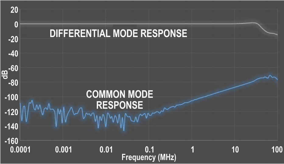
The differential-mode frequency response plot was taken by applying a differential input voltage at the two input terminals (IN+ and IN–).
 |
|
| Figure 2. | Frequency response for differential and common mode signals. |
The gain resistors become part of the input resistance for the source. This provides better noise performance than the non-inverting configuration but limits the flexibility in setting the input impedance separately from the gain.
For the common-mode frequency response plot, the common-mode voltage is applied at two non-inverting input terminals (VREF) with IN+ and IN– tied together.