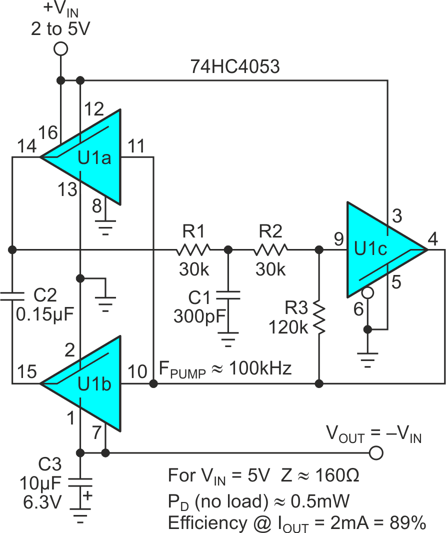
It’s interesting, useful, and fun that basic electronic topologies often turn out to have utility in multiple and surprisingly different applications. Figure 1 shows an example of such a circuit. It’s a charge pump voltage inverter circuit originally published in “A simple, accurate, and efficient charge pump voltage inverter for $1” (Ref. 1).
 |
|
| Figure 1. | Basic voltage inverter circuit scaled for efficiency at 100 kHz and several milliamps of current output. |
Configured thusly for the voltage inverter application, the pump is simple and cheap. It draws only about 1 µA per kHz (unloaded) from the 5-V rail.
An interesting variation results if pump capacitor C2 is reduced by several orders of magnitude. This makes the current pumped directly proportional to oscillator frequency:

Starting from that idea, then adding some simple discrete components, our original inverter circuit becomes the core of an inexpensive, fast (1 MHz), low power voltage to frequency converter. Figure 2 shows how.
 |
|
| Figure 2. | Modified voltage inverter becomes power thrifty 1 MHz VFC. |
Input current = VIN/R1 charges C3 which causes transconductance amplifier Q1, Q2 to sink, increasing current from Schmidt trigger oscillator cap C1. This increases U1c oscillator frequency and the current pumped by U1a,b and C2. This is because the pump current has negative polarity (remember we started with a voltage inverter circuit); it completes a feedback loop that continuously balances pump current to equal input current:
Q3 provides the ramp reset pulse that initiates each oscillator cycle. R6 limits C2 discharge current to prevent driving U1 pin 1 substrate diodes into conduction, which could steal a fraction of IPUMP and thus create nonlinearity. The ratio of R5/R3 is chosen to balance Q2/Q1 collector currents at VIN and FPUMP equal zero, thus minimizing VIN zero offset. Consequently, linearity and zero offset errors are less than 1% of full-scale.
However, this leaves open the possibility of unacceptable scale factor error if the +5-logic power rail isn’t accurate enough.
What if we want a precision voltage reference that’s independent of +5 instability? Figure 3 answers that question.
 |
|
| Figure 3. | U2 shunt reference stabilizes C2 charge to a +5 independent precision 2.50 V. |
Adding the reference does, however, increase parts cost by about half a buck and max power consumption by about half a milliamp. These totals are still rather reasonable prices to pay for accurate and fast conversions. Yes, for a VFC, 10-bit resolution in a millisecond is pretty fast.
Note that R1 can be chosen to implement almost any desired VIN full-scale factor.
Reference
- Woodward, Stephen. “A simple, accurate, and efficient charge pump voltage inverter for $1.”