Pulse width modulation (PWM) is a terrific basis for digital to analog conversion. Credit goes to features like simplicity and (theoretically) perfect differential and integral linearity. Unfortunately, PWM’s need for ripple filtering tends to make it slow, especially if high resolution (upward of 8 bits) is required.
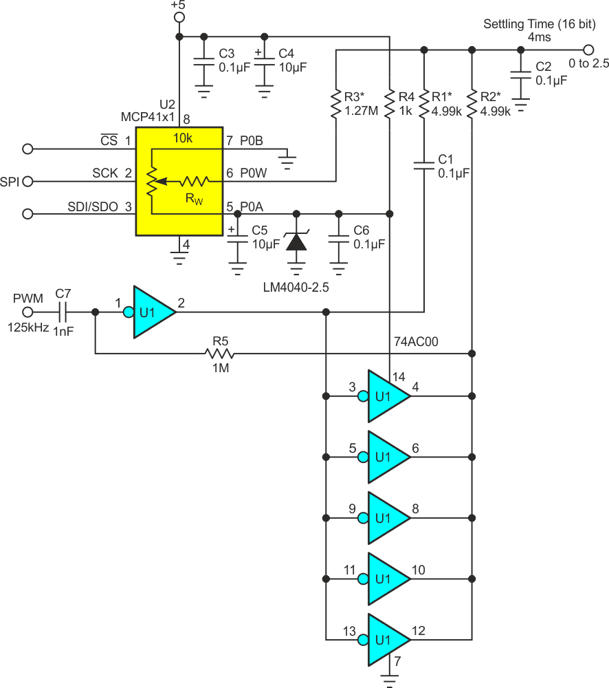
Figure 1 offers a workaround for PWM’s lethargy by using it to implement only the most significant 8 bits of a high resolution (16-bit) DAC while a different technology (digital potentiometer) provides the low order 8. The two outputs are then passively summed in a simple 256:1 ratio resistor voltage divider. The payoff is 256 times faster settling (than if PWM were used for a full 16-bit count), combined with 16-bit resolution, monotonicity, linearity (both INL and DNL) and microvolt zero stability. The circuit lives off just a few mA drawn from a single 5-V rail while incorporating a pretty good voltage reference. And it’s cheap.
 |
|
| Figure 1. | PWM most significant byte (msbyte) combines with Dpot least significant byte (lsbyte) to provide 16-bit resolution, monotonicity, and linearity. |
Incoming 3 to 5-V logic, 8-bit resolution PWM is inverted and level-shifted by R5C7 and high-speed AC inverter U1 to become an accurate 0 to 2.50 V square wave thanks to the LM4040 voltage reference and the inherent properties of CMOS logic when used as precision analog switches. The waveform is un-inverted and buffered by the other five elements of U1 to become a low impedance (~5 Ω) high quality 0 to 100% duty cycle PWM output. U1’s excellent transition symmetry (TPHL and TPLH propagation times differ by less than 100 ps) helps promote accuracy and linearity while the positive feedback through R5 creates a latching action that accommodates static 0% (0 V) and 100% (2.5 V) duty cycle states.
Active low-pass analog-ripple-subtraction filtering occurs via the R1C1 + R2C2 network as described in “Cancel PWM DAC ripple with analog subtraction” (Ref. 1). The 4.99 kΩ x 0.1 µF = 499 µs RC time-constant shown is appropriate for 16-bit (96 dB) ripple attenuation if we assume an 256/32 MHz = 8 µs PWM period. The capacitances will of course need proportional adjustment for different PWM clock frequencies.
Meanwhile 1k Dpot U2 provides an SPI controlled, 8-bit resolution, 0 to 2.5 V lsbyte contribution that’s summed with the U1’s PWM output in a 256:1 ratio by the R2R3 voltage divider. The R2:R3 ratio should be accurate and stable to better than 0.5%. R3 is so much higher than the 2.5k (max) variable impedance provided by the pot that its contribution to nonlinearity stays less than ±½ lsb.
Meanwhile wiper resistance effects are so small as to be completely academic.
Reference
- Woodward, Stephen. "Cancel PWM DAC ripple with analog subtraction."