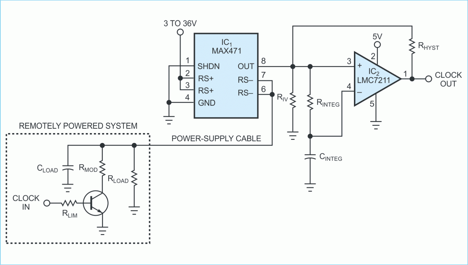
A high-side current-sense amplifier, IC1, offers a simple method of combining low-speed clocks or other signals with dc power in cables between subsystems (Figure 1). Designed for monitoring charge and discharge current in secondary batteries, IC1 outputs a current of 0.5 mA per amp of load current flowing through its internal sense resistor while rejecting common-mode supply-voltage noise. The on-chip sense resistor handles as much as 3 A of continuous current. The IC accommodates power-supply voltages from 3 to 36 V.
 |
|
| Figure 1. | By using a high-side current-sense amplifier IC (IC1) in an unconventional manner, you can combine clock or data signals with dc power in cables. |
Figure 1 depicts a subsystem that receives power from its host system and simultaneously transmits a clock signal back on the same wire. The circuit uses the clock in the remote system to modulate power-supply current via an open-collector driver or discrete transistor and RMOD, a switched load resistance. In the host system, IC1 develops a voltage across RIV, which represents the instantaneous sum of supply current and modulation current. RINTEG and CINTEG filter this voltage, biasing the comparator’s reference pin to a level that tracks average power-supply current. As the signal swings above and below this reference level, the comparator outputs the recovered clock. RHYST adds a small amount of hysteresis to ensure clean clock recovery.
IC2, which comes in an SOT23-5 package, is a CMOS comparator with a range. This range allows you to choose RIV with relative freedom – expect about 1 V/A of load current for each 2 kΩ of resistance. The input offset of low-grade versions of IC2, an LMC7211, can be as much as ±18 mV. Thus, select RMOD and RIV to produce 50 mV or more of modulation on RIV, and then choose RHYST to obtain a few additional millivolts of shift at this node when the comparator changes state. None of these values is critical.
For this scheme to work as expected, the power-supply current to the remote system must be relatively constant, except for the intentional modulation. Slow power-supply current variations do not cause problems, as long as you choose the integrator components with care. The integrator RC product should be about 10 times the clock period. It’s convenient to choose RINTEG of approximately 1 MΩ when using CMOS comparators, such as IC2. You can then use ceramic or plastic-film capacitors for CINTEG, thus minimizing the risk of failure due to capacitor leakage.
The circuit can also transmit data if the data contains little dc bias variation or if you replace the integrator components with a fixed bias source. This change means, of course, that no significant power-supply current change is allowable after calibration.
IC1’s output rise and fall times measure approximately 4 msec, a figure similar to IC2’s response-time specification. The remote system’s power-supply bypass capacitance may impose an upper bound on the clock rate because this capacitance limits the modulation rate of the supply current. This time constant is CLOAD × (RSENSE + RCABLE).
RSENSE is less than 0.07 Ω in IC1, and the cable’s series resistance depends on the application. You must add the equivalent series resistance of the power source, connectors, and any other associated resistive elements to RSENSE in this calculation if you’re pushing the envelope of the circuit’s performance.