At times, designers face a limited amount of wire and/or a limited cost to communicate with a remote device such as a sensor. Many devices allow communication over an ac or dc power line employing an AM or FM modulation scheme.
However, they tend to be costly. This design is a simple, low-cost method for sending data across the same wire used to supply power. It’s based on modulating current from a remote device back to a host. A later example shows how the host also can modulate voltage to the slave. The host decodes the data by sensing current changes to the slave and recovering the data with an analog comparator. The scheme will cause a small drop in the supply voltage to the remote device that is insignificant in most applications.
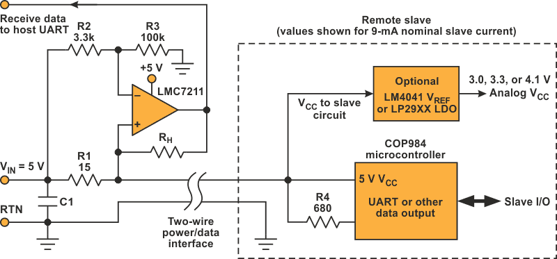
The remote microcontroller sends data by sinking current through an output port and series resistor to ground. The resistor value is chosen by calculating the maximum current required by the remote circuit and choosing a resistor that will increase the current required by an amount that can be easily measured with the shunt circuit shown (Fig. 1). Designers must ensure that normal operation of the slave doesn’t cause current excursions that get interpreted as data, or they must filter these conditions (explained later). Sometimes, hysteresis may be necessary and can be added with a bit of positive feedback.
The recovery circuit in Figure 1 uses a single comparator that senses the amount of current passing through the shunt resistor. If a UART is being used, such as provided in the COP984 8-bit microcontroller, the comparator is configured to provide a logic low when a data bit is on (mark). The comparator is biased with the divider R2/R3 so the data output from the comparator is stable logic high during normal no-data-flow operation. When a start bit is sent from the remote, the host senses the increase in current and the comparator drives a logic low into the host UART or other recovery device. When the output data is off, the output from the remote device is off and not sinking current.
The Figure 1 circuit employs a National Semiconductor LMC7211 comparator. The part was chosen because, unlike traditional comparators, the common-mode input range extends to the positive rail. This is required when sensing a voltage with a potential at or near the positive rail. Other reasons for selecting this part include its low operating voltage (down to 2.7 V), its push-pull output (saves a pull-up), and an extremely small SOT23-5 package.
This implementation has been optimized for a total slave current load of 9 mA. The comparator reference voltage is set at 4.84 V with R2 and R3. With VIN set at 5.0 V the drop across the shunt R1 will result in the voltage at the noninverting input being either 4.7 V when the signal from the microcontroller is off (high) or 4.77 V when the signal is on.
Many microcontrollers will operate properly with voltages as low as 2.5 V. In this example, the slave voltage will stay within 5% of the 5-V VCC if the slave doesn’t generate significant load change. Designers must consider the minimum and maximum slave current in choosing the bias resistor values, as well as the current variation generated by the internal operation of the microcontroller.
With this circuit, the slave current can vary from 6 mA to 10 mA without significantly affecting operation. Larger variations may require a larger shunt R1 (and thus a larger VCC drop) and an appropriate change in reference resistor R2. Fast transient current changes also may be filtered by adding hysteresis with a positive feedback resistor (RH = 47k) and/or by adding a filter capacitor (C1) from the noninverting input to ground (0.1 µF). Slave VCC decoupling capacitors must be carefully selected to ensure the total capacitance doesn’t distort the relatively slow current modulation. A value of 1 µF will limit the data frequency to about 10 kbits/s.
In some applications, slave circuits may not tolerate the VCC noise generated by the modulator. This may be seen in situations where a large variation occurs at the slave and an analog block is being employed. In these situations, either a voltage reference (such as an LM4040/4041) if the current required is limited or an LP2951 low-dropout regulator can be used if the current requirement is up to 100 mA (LP2952 or LP2960 for current up to 0.5 A). This regulator circuit is able to generate a stable voltage a few hundred millivolts below the lowest slave voltage or set at a standard fixed voltage of 3.0, 3.3, 4.1 V, etc.
The LMC7211 and LMC6772 feature delay times that enable them to be used for frequencies up to about 128 kbits/s, based on the value of the capacitor required at the slave. For higher-frequency applications, a faster device can be used. Also, the Figure 1 circuit may be used when operating with a 3-V power source.
 |
|
| Figure 1. | This recovery circuit operates by modulating current from a remote device back to a host. Here, a single comparator senses the amount of current passing through the shunt resistor. |
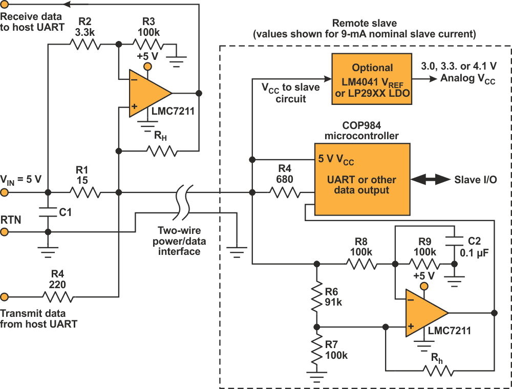
A bidirectional circuit also can be implemented by modulating the voltage from the host to the slave and modulating current from the slave back to the host. This design may require a greater variation in voltage to the slave to ensure adequate margins. The recovery circuit for the slave can employ the same single comparator. In this case, however, the comparator is looking at the absolute voltage change from the host.
In another configuration, a simple voltage divider (R1/R4) can modulate the voltage from the host to the slave (Fig. 2). The slave circuit simply compares the voltage being provided to the voltage stored in C2. The C2/R8/R9 time constant is set much longer than 8-bit times so the reference level will be stable for this worst-case situation. When the host sends a bit, R4 will pull the slave voltage down and the slave comparator will pass a logic low back to its UART or other receiving device. The host will see its own transmitted data looped back into its recovery circuit. This is typically ignored or can be used for error checking (compare transmitted to received data).
 |
|
| Figure 2. | A simple voltage divider (R1/R4) modulates the voltage from the host to the slave. The slave circuit compares the voltage being provided to the voltage stored in C2. |
These circuits are meant to be foundations for a circuit that will work in a particular system. They may not be optimum for a particular design, but by using the concepts and variations described, designers may implement this extremely small and low-cost communications scheme with great results.
