The CD4011 CMOS NAND gate has a typical input current of 10 pA at room temperature. You can charge a capacitor connected to the gate input with currents on the order of hundreds of picoamperes and neglect the influence of the gate-input current on the charging time of the capacitor. You normally need large-value resistors to limit currents to this low level. These resistors are not commonly available. You can instead use a transistor as a current attenuator, despite its more usual amplifying nature.
The circuit in Figure 1 uses one CD4011 package containing four NAND gates, which you can use to build four independent long-duration timers. Note, however, that temperature variations and component parameters affect the timing, a situation that may be acceptable if you are not concerned about accurate timing and need only a simple circuit without large-value electrolytic capacitors and resistors.
 |
|
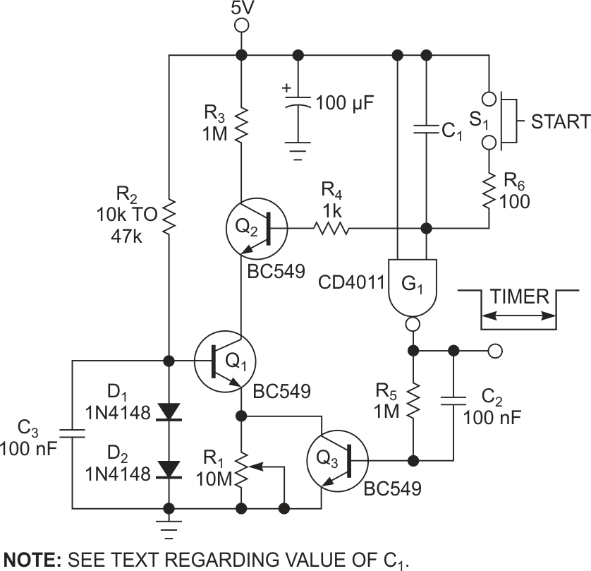
| Figure 1. | A constant-current source and current divider reduce the timing capacitor current to a low level to increase the charging time. |
The series-connected diode voltage drops of D1 and D2 bias current source Q1. The resulting voltage across R1 is a Q1 base-to-emitter-voltage junction drop less and sets the Q1 collector current, which is also the Q2 emitter current. The resulting Q2 base current is its emitter current divided by its current gain and charges timing capacitor C1.
Before the start of the timed period, the gate output is high, biasing on Q3 and Q1, allowing C1 to charge through the base-emitter junction of Q2. This action holds the gate input sufficiently below its switching threshold to maintain its high output state. Momentarily closing and then releasing S1 starts the timed period by discharging C1. This action drives the gate output low and ensures that Q3 is biased off, which allows Q1 and Q2 to slowly charge C1 through the constant-current action. The power-supply current draw of the gate increases somewhat as its input voltage pulls away from the 5 V rail.
When the C1 charge reaches the gate-switching threshold of approximately 2.5 V, the gate output begins to rise, turning on Q3. This action increases the current through Q1 and Q2, resulting in saturation of Q2 and a faster charging of C1. This positive feedback provides the necessary hysteresis to complete the charging of C1 and return the gate output high.
Linearity with changes in R1 is impossible due to variations in the transistor’s current gain. The built and tested circuit does exhibit linearity with the value of timing capacitor C1, which you can choose experimentally for the required time. Once you determine a time for a short interval, such as that for a 10- or a 100-nF capacitor, you can use this knowledge to scale to longer timing. In the tested circuit, with R1 set to 1 MΩ, a C1 value of 10 nF results in a time of 10 sec; a C1 value of 100 nF increases the time to 100 sec.
Editor’s notes:
Constructing a low-current circuit is challenging. Some types of PCB-soldering flux can become conductive, wreaking havoc with what should be a tiny current. Consider “open-air” connection of the Q1-emitter collector and the Q2-emitter base leads to remove them from the board.
Transistor-leakage currents and current gains vary widely from device to device and with temperature. This variation can drastically affect the expected low-level current and capacitor charge time. Although the CD4011’s typical input current is 10 pA at room temperature, it could be as high as 100 nA and increase to 1 μA at high temperature. Likewise, the transistor collector-to-base leakage could be a maximum of 15 nA at room temperature and 125 μA at high temperature, and it approximately doubles for every 10 °C rise in temperature. It might be necessary to hand-select transistors and CD4011 inputs or devices to overcome this problem. Also, remember to tie any other unused CD4011-gate inputs to ground or 5V to avoid floating-input problems.
Do not set R1 so low that Q1 or Q2 saturates during the timed period; they must remain in their linear region as set by the value of the Q2 collector resistor. Timing capacitor C1 should have a high-quality, low-leakage dielectric, such as polyester; check the leakage specifications of the size and type you intend to use for suitability with the low-level current.