An electronic dice is always an enjoyable project, which is easy to implement with some lines of program code on a microcontroller, or with a few digital components. However, implementing an electronic dice in analog technology is more of a challenge. The circuit displayed here realizes a fully analog electronic dice with a limited number of components and can be implemented on a small PCB. A variety of interesting analog techniques are used, making this an interesting application.
The heart of the circuit, shown in Figure 1, is situated around the three op amps at the top of the schematic. These op amps form a periodic analog staircase voltage, with six analog levels, corresponding to the states of the electronic dice. From left to right, we see the clock oscillator, a charge pump and a reset circuit for this charge pump. We will now discuss those parts in that order.
 |
|
| Figure 1. | The analog electronic dice circuit, from left to right, shows the clock oscillator, a charge pump, and a reset circuit for this charge pump. |
Leftmost, a relaxation oscillator is formed around IC1A. This is a classic circuit, modified for a single supply voltage, setting the bias halfway that of the supply voltage with voltage divider R3 and R8. The oscillation frequency is chosen by means of C1 and R1. The output of the oscillator is a symmetric square wave. The role of Q2 will be discussed later; consider Q2 inactive for now.
The oscillator drives a charge pump, formed around IC1B. At each falling edge of the square wave, most of the charge of C2 is transferred into C3 via diode D1, producing a step in the staircase voltage that appears at the output of IC1B. During the rising edge, C2 is charged again via D2. Thanks to the reverse biased diode D1, recharging C2 does not influence the output of the charge pump.
After the staircase voltage has made six steps, we need to reset the charge pump and restart the cycle. Imagine that at step #7, we cross a certain threshold level and then we immediately discharge C3, so step #7 lasts for an extremely short time. The comparator around IC1C performs this role. The threshold voltage is set by voltage divider R7, R6.
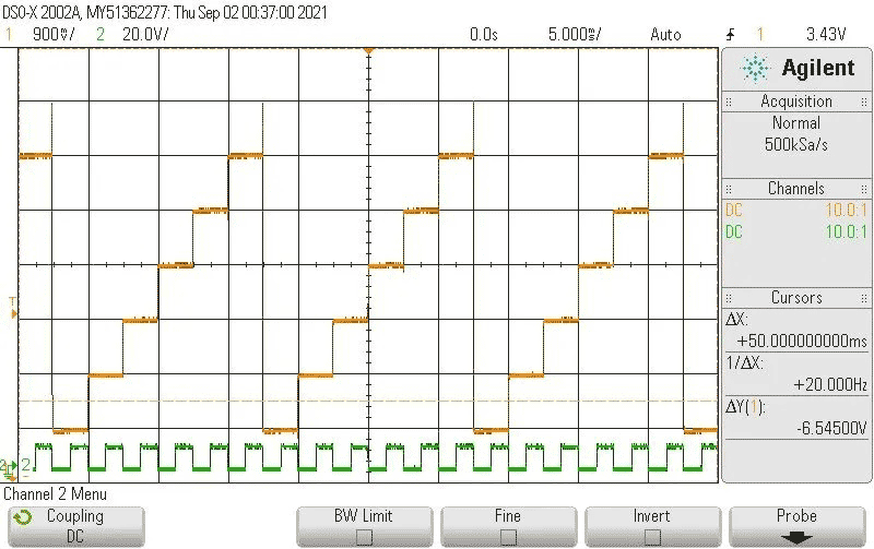
However, some details are important here: D3, R4 and C4 cause a small delay for a rising edge, but a larger delay for a falling edge. This allows the reset circuit to react promptly when step #7 arrives but at the same time, this reset action is held for enough time to fully discharge C3. The actual discharge action is performed by driving transistor Q1 into saturation. The result is shown in Figure 2.
 |
|
| Figure 2. | Staircase voltage and clock. |
On top is the staircase voltage and underneath, the clock signal. Note, changes occur only at the falling edge of the clock. When the clock is high, the staircase voltage is always stable. Importantly, closing switch S1 will halt the oscillator, but thanks to Q2 this can only happen when the clock level is high. This means, if you “roll the dice,” the oscillator stops on a stair of the waveform and never in between the stairs. Hence, when S1 is pressed, the level is always a well-defined analog voltage, selected at random, out of a set of six possible voltages.
Importantly, when stopping the oscillator, the probability of each analog voltage level is exactly 1/6 because everything follows the master clock, and this clock can only be held when its state is high. In other words, at the time the oscillator stops, all transitions are already over. The charge pump update actions start at the falling edges of the clock; hence by the time you can stop the oscillator, the last update action is surely completed.
To display the result, we use five comparators, controlling the LEDs. The resistors R9 through R14 form a tapped voltage divider, creating five comparison levels, which are halfway the staircase steps. The comparison level at pin 9 of IC2C is shown as an example in Figure 3.
 |
|
| Figure 3. | Example of an LED decoder comparison level. |
In this way there is margin for component tolerances, as well as for some drift of the voltage when you want to hold the value for a long time. However, as IC1 is a CMOS op amp, it has very low leakage currents and therefore the output voltage can be held for many minutes without any change visible on the scope.
The decoder for the LED states uses the remaining IC1D op amp and four op amps from an LM324. Some optimizations were performed to reduce the size of the decoding circuit. Here it is important to understand that with a rising voltage, the sequence of numbers does not have to be 1-2-3-4-5-6-repeat; a different order is fine too. For the sake of decoder simplicity, the sequence was chosen to be 1-3-5-6-4-2-repeat. The Table 1 will make this idea clear. Imagine going through the states in the order as listed, starting with all LEDs off and reading the changes.
| Table 1. | Changes in LED states | |||||||||||||||||||||||||||||||||||||||||||||||||
|
||||||||||||||||||||||||||||||||||||||||||||||||||
At this point, the main working principles of the fully analog electronic dice have been explained but one more detail is to be found in R18, R21. Without this voltage divider, LED4 does not fully dim due to the load on op amp IC2B. This op amp indeed sources current in LED3 and LED7 too, causing a voltage drop at the output.
The final part to explain is the LED blanking circuit. If IC2 was always powered, the LEDs would also light while the oscillator is running. We prefer the LEDs to light only when S1 is pushed, and therefore supply power to IC2 only in that case. This happens via T1 and R24. However, when IC2 is not powered, we should limit the current at its inputs, which is the sole purpose of resistor R25. IC2 also needs to be a bipolar op amp, to avoid problems with the power-off state, which is why a classic LM324 was chosen.
In the implementation some values are critical. All resistors should have 1% tolerance, except those in series with the LEDs, which can be less precise. Ideally, capacitors C2 and C3 should also have only 1% tolerance, which is difficult or more expensive to obtain. A scope measurement of the staircase voltage on the output of op amp IC1B will show less than six steps if the ratio C3/C2 is too low, or more than six steps if that ratio is too high. A one-time adjustment can be made experimentally by putting a smaller capacitor in parallel to C2 or C3, for decreasing or increasing the ratio, respectively.
In this circuit design all critical internal voltages are proportional to the supply voltage. Therefore, when accurate component values are used, the circuit operates reliably on a 9 V battery, even if the battery is discharged down to 7 volts.
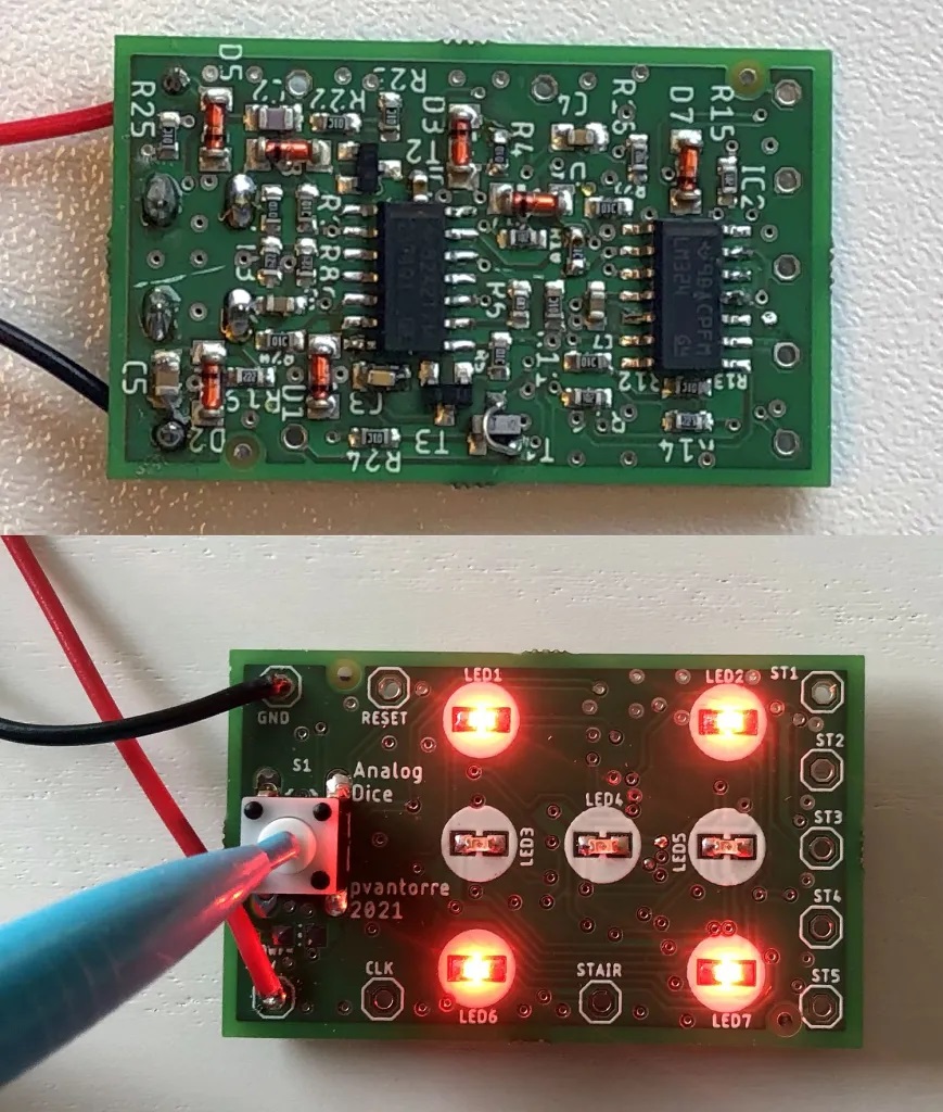
A small PCB was manufactured, as illustrated in the Figure 4 and in the video (Reference 1).
 |
|
| Figure 4. | An analog electronic dice assembled on a PCB. |
In this video the blanking is inactivated, by bypassing T1; therefore the LEDs also light while the oscillator is running. With the blanking active, the LEDs do not light until the S1 button is pressed.
The measured standby current with blanking active is 3.8 mA in standby and 13.8 mA when a “six” is displayed. With blanking active, it is probably interesting to add a power-on LED in a different color, as an indication that the electronic dice is switched on, and in standby to show a random number.
