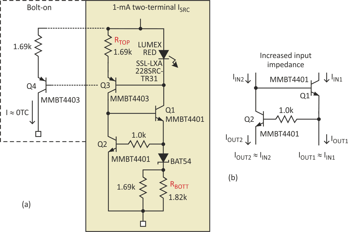
A two-terminal current source using the basic circuit of Figure 1a can be enhanced by adding on an independent subcircuit that uses degeneration of a PNP transistor to achieve zero temperature coefficient (tempco or TC). This low-cost design is the result of collecting data on many semiconductor devices over a 15+ year period and frequent reviews of the data. ("Degeneration" is the insertion a resistor in series with the emitter, which decreases the gain of the amplifier but improves attributes such as linearity and input impedance.)
The key semiconductors in the bill of materials (BOM) of Table 1 are critical to this circuit, so design and test only with these parts. The choice of parts and their vendor makes this design viable, and the circuit has been built over various lots of material with parts purchased from different distributors. Both the MMBT4401 and the MMBT4403 transistors should each come from their own, single tape reel of parts.
| Table 1. | BOM of key parts | ||||||||||||||||||||||||||||||
|
|||||||||||||||||||||||||||||||
Audio-design engineers have known for years that ON Semiconductor’s MMBT4401 and MMBT4403 feature very low base resistance (RB) and thermal noise, and are very good for current-source and mirror circuits. The MMBT4401 and MMBT4403 are complementary devices related to dc biasing and tempco. Complementary devices make it easier to understand the zero tempco design as a “glue” circuit needs to pass the current from the PNP device Q3 of its mirror to Q2. The base-to-emitter voltages VBE will be approximately equal in those two transistors.
The design is fault-tolerant and can be reverse-biased. For industrial designs at higher supply voltages, the majority of the forward voltage drop is across the collector/base of Q1 and Q3, the top MMBT4401 and MMBT4403 devices, with a 40-V BVCBO (the collector-to-base breakdown voltage with open-circuit emitter). A series resistor can be used for surge protection, with a penalty in voltage headroom.
A compact printed-circuit-board (PCB) layout is needed to prevent thermal gradients. The LED "photoelectric effect" has been found to not be an issue here, as the LED is the type where the LED lens is pointing down when mounted in the PCB. Light-tolerance testing has also been performed. Viewing the LED from the die-mount side of its package shows a red glow and can be used as a visual indicator that the current source is functional.
Figure 1b is the “glue” circuit using two each of MMBT4401 NPN devices and 1.0-kΩ resistor. It connects a top current mirror and a bottom current mirror. The two key design equations for the add-on circuit are:
IE(Q2) ≈ IIN2, therefore:

IOUT1 ≈ IC(Q1), therefore:

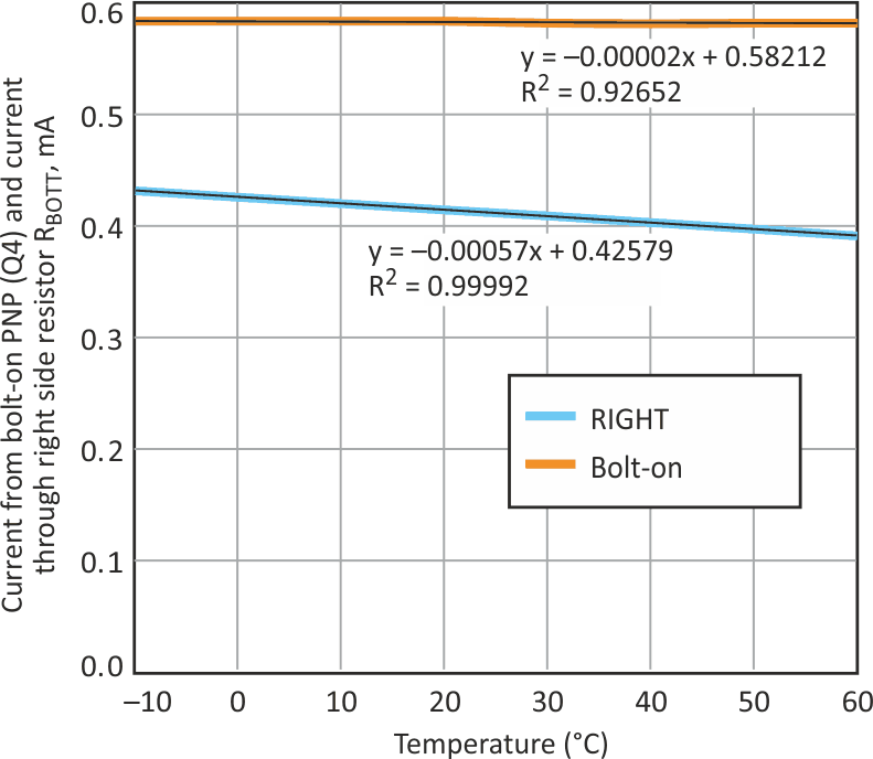
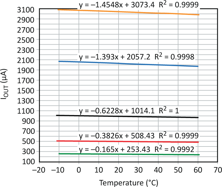
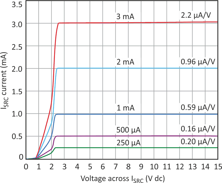
Figure 2 shows the current-source values and their change with temperature, while the steady-state performance over input voltage and the minimum operating conditions are shown in Figure 3. The tempco of the bolt-on circuit (Figure 4) compares favorably with the REF200, a commercially available, precision, dual-current source/current sink. That device has a temperature coefficient of ±25 ppm/°C on its fixed 100-μA current source.
However, this current source can be set to any desired current and costs significantly less than the REF200. Also, the typical capacitance of the REF200 is 10 pF, while the value for this current source is less than 10 pF, and the typical output impedance of a REF200 is 100 MΩ from 2.5 V to 40 V. The two-terminal current source is a very repeatable, low-cost circuit and is a viable choice for replacing certain commercial ICs providing the same function.
 |
|
| Figure 4. | The plot indicates ~0 tempco in the bolt-on MMT4403 (Q4) PNP transistor to the 1-mA ISRC. The red plot line for the bolt-on shows a TC of –35 ppm/°C. |


