Variable regulated power supplies are handy tools found on well-equipped electronics lab benches. The symmetrical varieties that produce equal voltage outputs of opposite polarity, are even more so. Figure 1’s version of a symmetrical 0 V to 10 V, 1.5 A lab supply implements an extra handy trick: computer programming via a single PWM output.
 |
|
| Figure 1. | LM337, LM317, and CD4053 join forces in a symmetrical 0 to ±10 V PWM programmed power supply. |
In Figure 1’s PWM DAC interface, DPST switches U1a and U1b accept a 10-kHz PWM 5-V signal to generate a +1.25 V to -8.75 V “ADJ” control signal on C2 for the U2 regulator. VOUT = ADJ – 1.25 V, so ADJ = 1.25 V forces an output of zero and U3 follows along. At the other end of the span, ADJ = -8.75 V makes them make 10 V. Current source Q1 reduces zero offset error by (mostly) nulling out the 65 µA (typical) 337 ADJ pin bias current.
Inverter switch U1c provides active ripple filtering via analog subtraction. Other PWM frequencies can be accommodated by proportional scaling of filter caps C1 and C2.
The feedback loop established by R2 and R3 makes the 10 V full-scale outputs proportional to U2’s precision internal reference. This makes output voltage an accurate function of PWM duty factor D with functionality (D ranging from 0 to 1) given by…

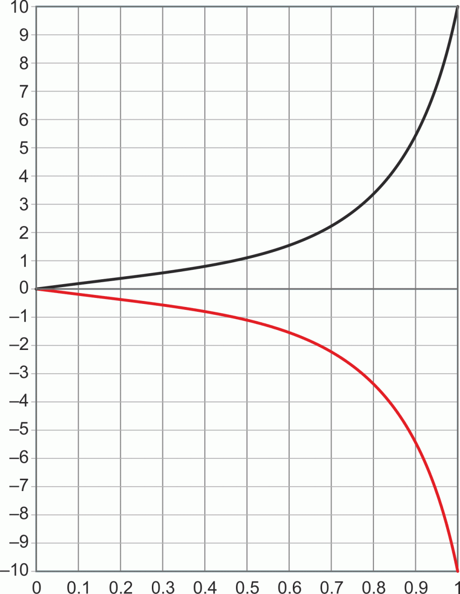
…as graphed in Figure 2.
 |
|
| Figure 2. | VOUT (0 to –10 V and +10 V) versus PWM duty factor, D (0 to 1). The black curve is LM317’s VOUT = 1.25 D/(1 – 0.875 D). The red curve is LM337’s VOUT = –1.25 D/(1 – 0.875 D). |
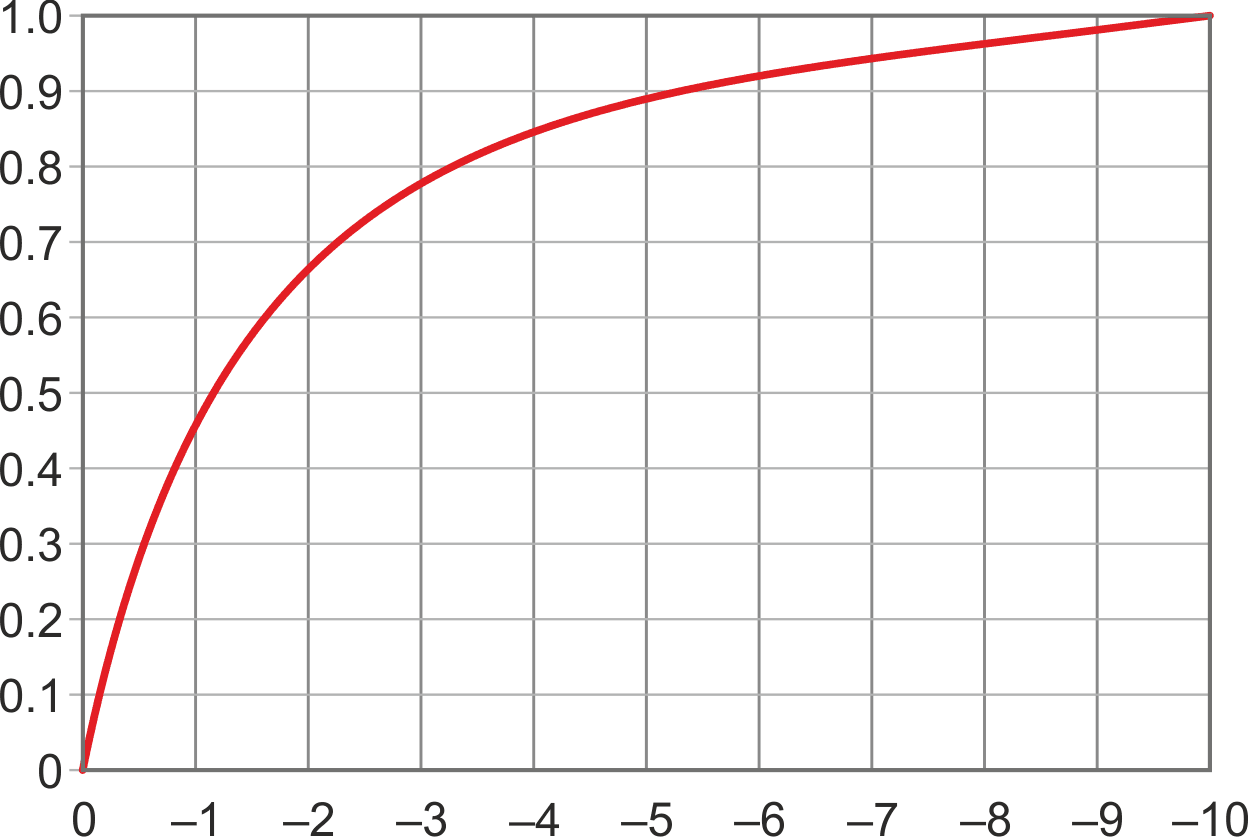
Figure 3 plots the inverse of Figure 2, yielding the PWM D required for any desired VOUT.
 |
|
| Figure 3. | The PWM D required for any desired VOUT. PWM D = |VOUT|/(0.875 |VOUT| + 1.25). |
For the corresponding 8-bit PWM setting:

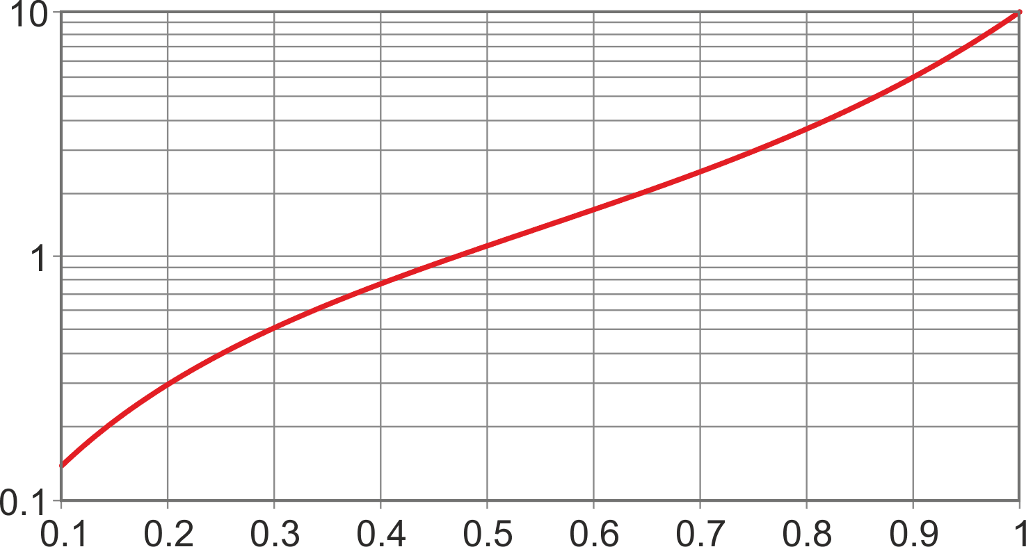
Actually, as shown in Figure 4, the VOUT-to-D relation is surprisingly close to logarithmic.
 |
|
| Figure 4. | D (x-axis) versus VOUT (y-axis) is (fairly) close to a logarithmic function, which makes good use of limited 8-bit PWM resolution. |
The supply rail inputs must be at least 13 V to accommodate U2’s and U3’s minimum headroom requirement. The negative input is limited to a 15 V max in recognition of U1’s 20-V absmax rating.
U2’s 0 to –10 V output is inverted by the Q2, Q3, and Q4 differential amplifier via feedback to U3’s ADJ input, forcing U3 to track U2. This results in the symmetrical outputs plotted in Figure 2. Q5 provides U3’s minimum output load while R6 does that job for U2.
U2 and U3 must of course be adequately heatsunk as dictated by their power dissipation which is equal to output current multiplied by the VIN to VOUT differential. Maximum heating (up to 20 W) therefore occurs at high current and low voltage.