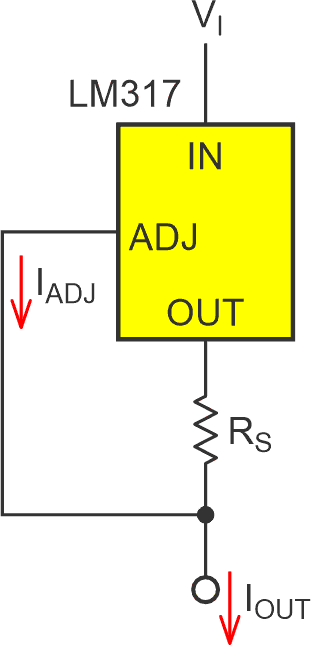
LM317 fans will recognize Figure 1 as the traditional LM317 constant current source topology. It closely regulates IOUT = VADJ/RS by forcing the OUTPUT pin to be VADJ = 1.25 V positive relative to the ADJ pin. Thus, IOUT = VADJ/RS to a very good approximation. Master chip chef Bob Pease cooked it up to be so!
 |
|
| Figure 1. | Classic LM317 constant current source, IOUT = VADJ/RS + IADJ ≈ ≈ VADJ/RS = 1.25/RS. |
In usual practice, IOUT >> IADJ, the latter being specified at 50 µA typical, 100 µA max. This simplifies the math by making the IADJ bias current safely ignorable without letting accuracy take a hit. It’s worked great for 50 years but it has an obvious downside: the way you program IOUT is by changing RS.
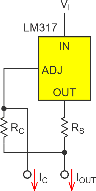
Figure 2 shows a new(er) topology with a different (more agile) method for making IOUT programmable.
 |
|
| Figure 2. | A novel LM317 topology enables control of amps of IOUT with just milliamps of IC, IOUT = (VADJ – (IC – IADJ)RC)/ RS – IC + IADJ ≈ (VADJ – (IC – IADJ)RC)/RS. |
Typically, RC > 100RS, making Figure 2 able to control up to 1.5 A of IOUT with just milliamps of IC. Of course, now it may no longer be good enough to just ignore IADJ.
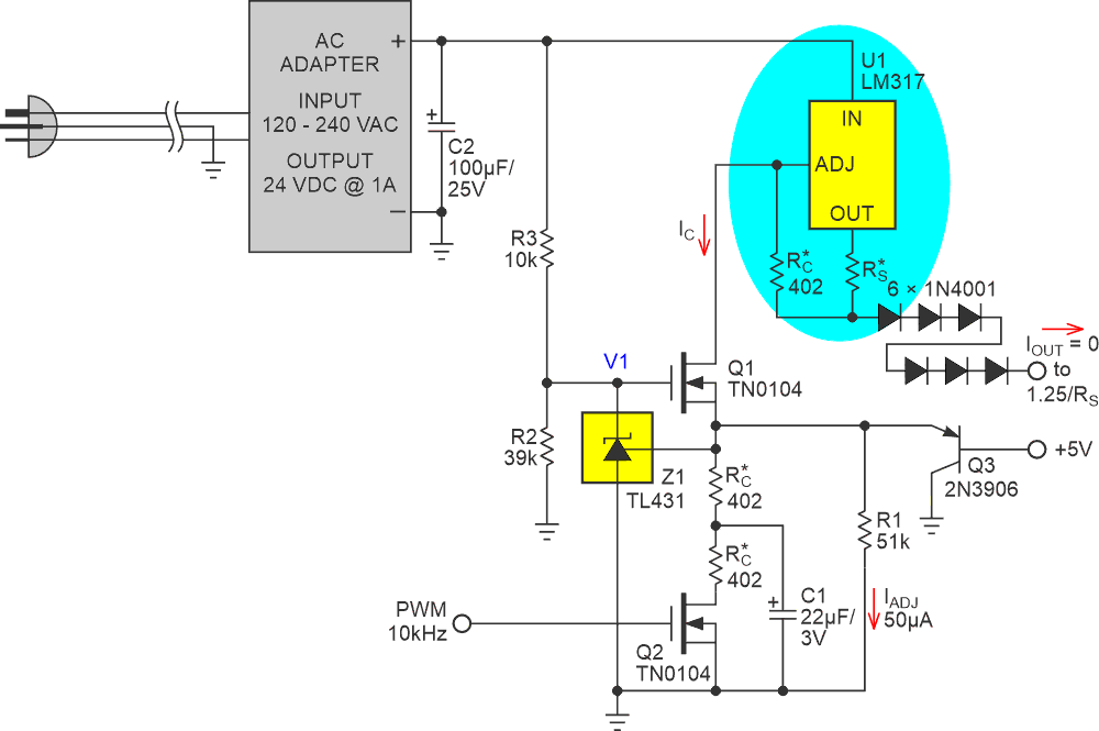
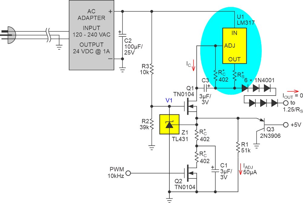
Figure 3 shows the idea fleshed out into a complete PWM controlled 15 V, 1 A, grounded-load current source that includes IADJ compensation. Here’s how it works.
 |
|
| Figure 3. | The 1-A, 15-V, PWM-programmed grounded-load current source with a novel LM317 topology. The asterisked resistors are 1% or better and RS = 1.25 Ω. |
The 5-Vpp PWM input has a frequency (FPWM) assumed to be 10 kHz or thereabouts. If it doesn’t, scale C1 appropriately with:
The resulting PWM switching of Q2 creates a variable resistance averaged by C1 to
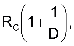
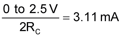
where D = the 0 to 1 PWM duty factor. Thus a
current
flows into Z1’s summing point.
Z1 servos the V1 gate drive of Q1 to hold its source at an accurate 2.5-V reference for the PWM conversion and to level shift IC to track U1’s ADJ pin. Also summed with IC is IADJ bias compensation (2.5v/51k = 50 µA) provided by R1.
The unsightly stack of six 1N4001’s is needed to provide bias for Q1 to work into. I freely admit that it’s not very pretty. Hopefully the novelty of Figure 2 makes up for it!
Note that accuracy and linearity mostly depend only on the match of the RC resistors and the precision of the Z1 and U1 internal references. It’s a happy coincidence that the 2:1 ratio of the TL431’s 2.5-V versus the LM317’s 1.25 V permits the convenient use of three identical RC resistors.
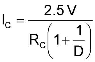
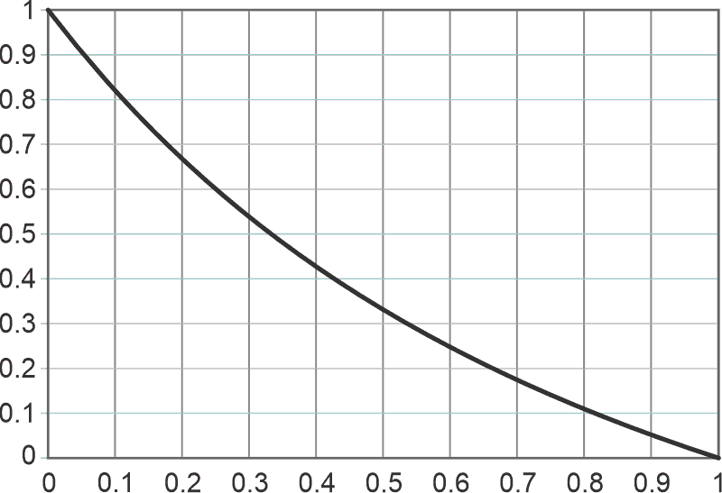
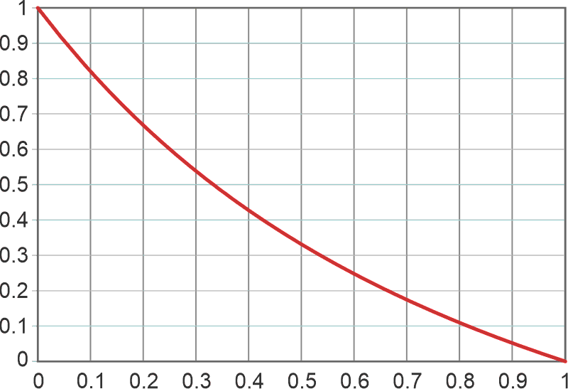
If RS = 1.25 Ω, then IOUT(MAX) = 1 A and IOUT versus D is as plotted in Figure 4.
 |
|
| Figure 4. | IOUT versus D where D (x-axis) is the PWM duty factor and IOUT (y-axis) is VADJ/1.25 = 1 A full-scale = 1 – 2/(1 + 1/D). |
D versus IOUT is plotted in Figure 5.
 |
|
| Figure 5. | D versus IOUT where IOUT (x-axis) is 1 A full-scale and D (y-axis) = 1/(2/(1 – IOUT) – 1). |
Note that U1 might be called upon to dissipate as much as:
- 20 W if RS = 1.25 Ω and IOUT(MAX) = 1 A
- 30 W if RS = 0.83 Ω and IOUT(MAX) = 1.5 A
Moral of the story: don’t be skimpy on the heatsink! Also note that RS should be rated for a wattage of at least 1.252/RS.
Then there’s the consideration of power up/down transients. When the system is first switched on and C1 is sitting discharged, and the controller will have about 4 to 8 milliseconds to initialize the PWM logic to 1.0 before C1 can charge enough to allow U1 to come on and start sourcing current. Don’t forget this detail during software development! On power-down, Q3 kicks in when +5 V drops below ~2 V. This saturates Q1 and forces IOUT to zero to protect the load as well as discharging C1 in preparation for the next power-up.
In closing
Thanks go (again) to savvy reader Ashutosh for his suggestion (Ref. 1) that the Figure 2 topology might deserve a focused DI of its own, and (likewise again) to editor Aalyia for the fertile DI environment she has created that makes this kind of teamwork, well, workable!
 |
|
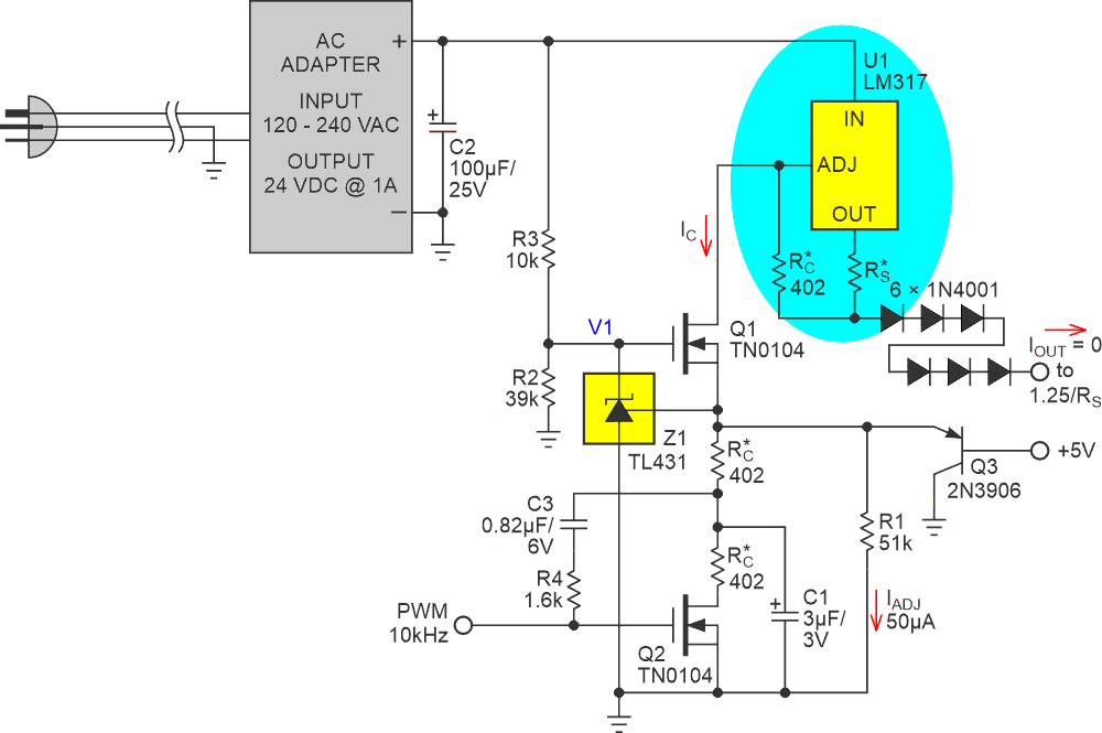
| Figure 6. | C3 adds 2nd order PWM ripple filtering for ~500% faster settling time. Thanks go to frequent contributor Christopher R. Paul for the comment that suggested it. |
 |
|
| Figure 7. | Analog ripple subtraction (Ref. 2) via R4 provides another method for 2nd order PWM ripple suppression. Thanks to commenter Val Filimonov for the suggestion! |
 |
|
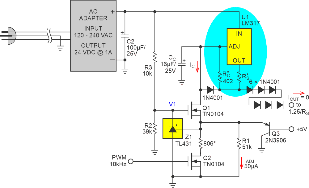
| Figure 8. | A contribution from frequent contributor Christopher R. Paul suggests improving PSRR with capacitor CC as well as making programming linear in D. For applications in which settling time isn’t important, this is a useful modification. Thanks, Chris. |
References
- Woodward, Stephen. "1 A, 20 V PWM DAC current source with tracking preregulator."
- Woodward, Stephen. "Cancel PWM DAC ripple with analog subtraction."
