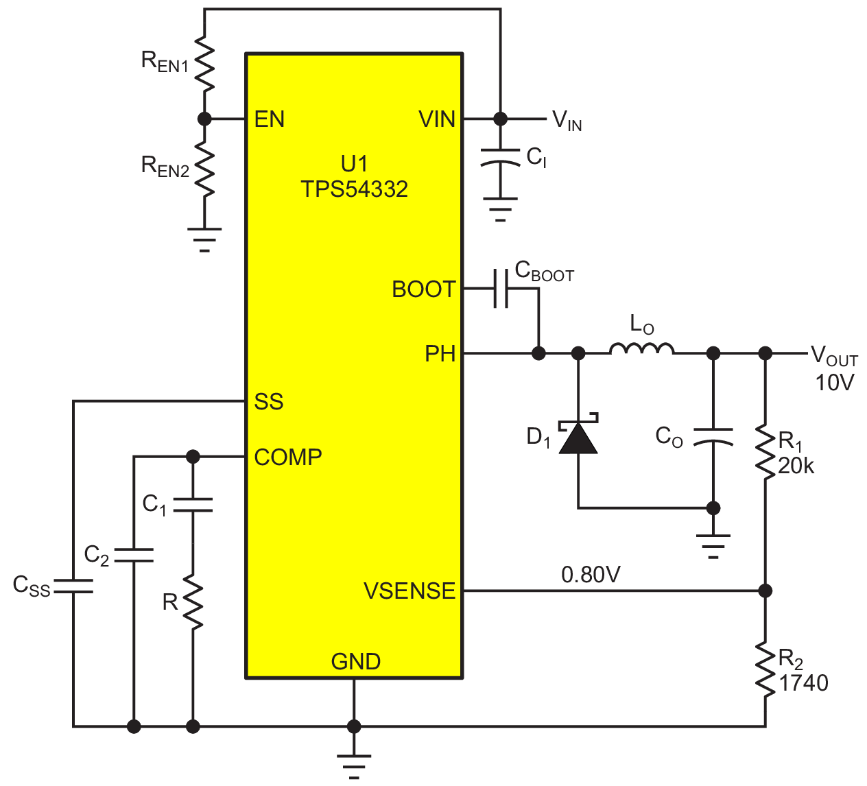
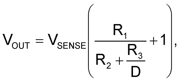
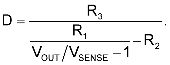
It’s remarkable how many switching regulator chips use the same basic two-resistor network for output voltage programming. Figure 1 illustrates this feature in a typical (buck type) regulator. See R1 and R2 where:
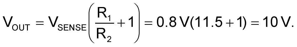
Quantitatively, the VSENSE feedback node voltage varies from type to type and recommended values for R1 can vary too, but the topology doesn’t. Most conform faithfully to Figure 1. This defacto uniformity is useful if your application needs digital control of VOUT via PWM.
 |
|
| Figure 1. | A typical regulator output programming network with a basic two-resistor network for output voltage programming. |
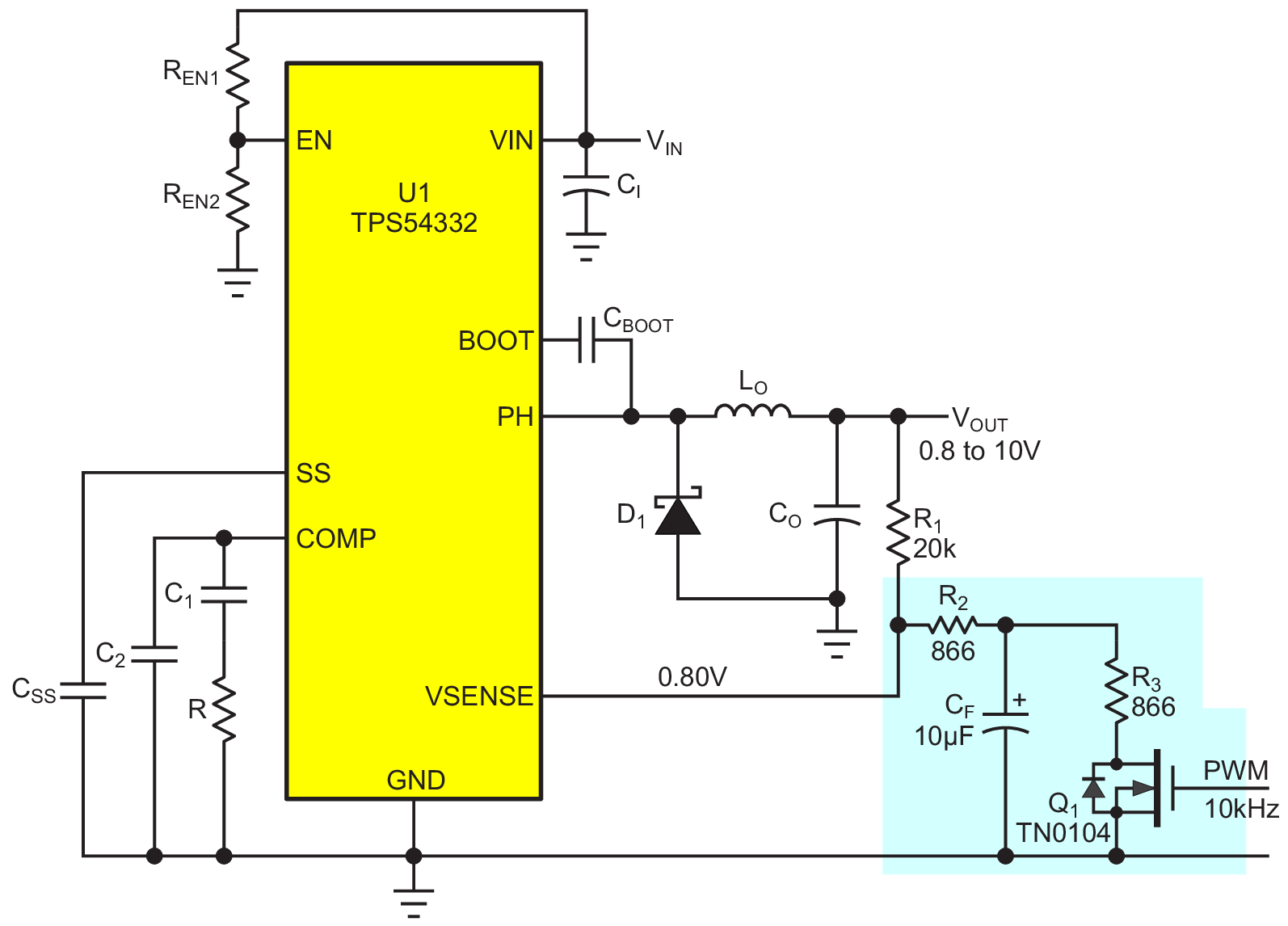
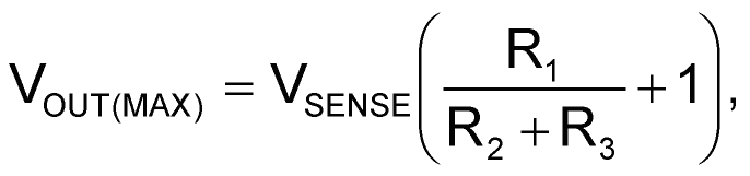
Figure 2 shows the simplistic three-component solution it makes possible where:
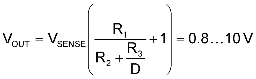
as D = 0 to 1.
 |
|
| Figure 2. | Simple circuit for regulator programming with PWM where VOUT ranges from 0.8 V to 10 V as the duty factor (D) goes from 0 to 1. |
All that’s required to add PWM control to Figure 1 is to split R2 into two equal halves, connect filter cap CF to the middle of the pair, and add PWM switch Q1 in series with its ground end.
The CF capacitance required for 1-LSB PWM ripple attenuation is 2(N-2)TPWM/R2, where N is number of PWM bits and TPWM is the PWM period. Since CF will never see more than perhaps a volt, its voltage rating isn’t much of an issue.
A cool feature of this simple topology is that, unlike many other schemes for digital power supply control, only the regulator’s internal voltage reference matters to regulation accuracy. Precision is therefore independent of external voltage sources, e.g. logic rails. This is a good thing because, for example, the tempco of the TPS54332’s reference is only 15 ppm/°C.
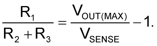
Figure 3 graphs VOUT versus the PWM D for the Figure 2 circuit where the X-axis is D, the Y-axis is VOUT and,

 |
|
| Figure 3. | Graph showing VOUT versus the Figure 2 PWM D. |
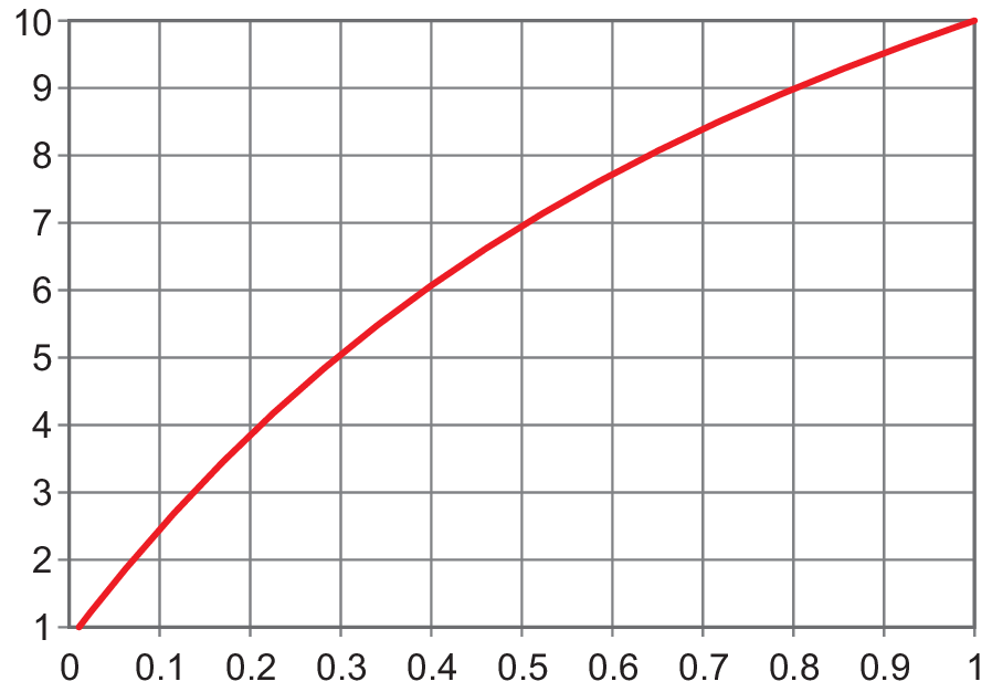
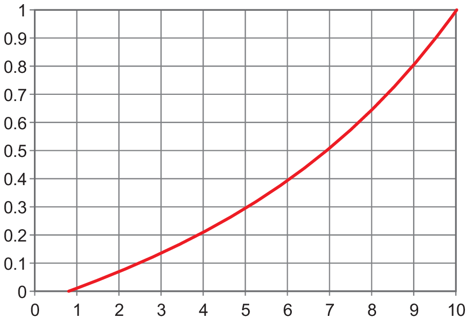
Figure 4 plots the inverse function with D vs VOUT where,
 |
|
| Figure 4. | D versus VOUT; the non-linearity necessitates a bit of software complexity to perform the conversion. |
The nonlinearity of D versus VOUT does incur the cost of a bit of software complexity (two subtractions and three divisions) to do the conversion. But since it buys substantial circuitry simplification, it seems a reasonable (maybe zero) cost. Or, if the necessary memory is available, a lookup table is another (simple!) possibility.