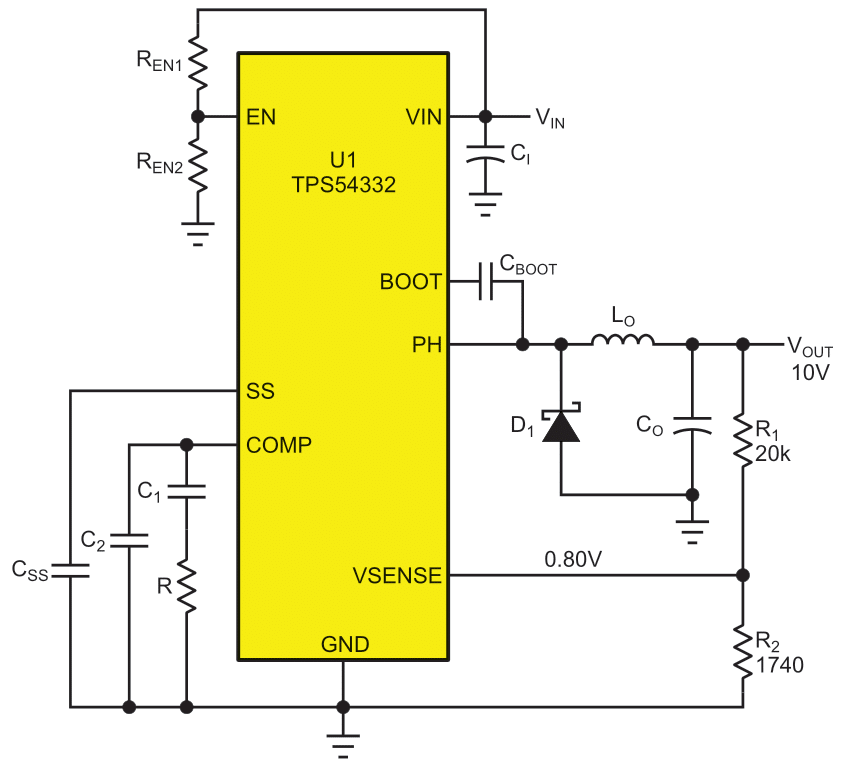
Whether its buck, boost, or buck/boost, internal or external switch, milliamps or tens of amps, a literal cornucopia of programmable output switching regulator/converter chips are commercially available. While the required external Ls and Cs (of course) vary wildly from topology to topology and chip to chip, (almost) all use exactly the same basic two-resistor network for output voltage programming shown in Figure 1. Its example buck type regulator was picked more or less arbitrarily, so please ignore the L and Cs and just focus on R1, R2, and (later) R3.
 |
|
| Figure 1. | The (almost) universal regulator output programming network where VOUT = VSENSE(R1/R2 + 1) = = 0.8 V × (11.5 + 1) = 10 V. |
For reasons known only to gurus of the mystic and marvelous monolithic realm, the precision VSENSE feedback node voltage varies from type to type over a roughly 3:1 range from 0.50 V to 1.5 V. Recommended values for R1 vary too.
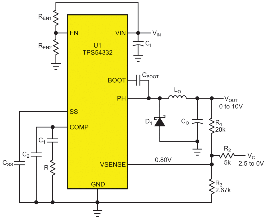
The point is the topology doesn’t vary. All (or at least most) conform faithfully to Figure 1. This surprising uniformity becomes very useful if your application requires DAC control of the output voltage. See Figure 2 for how this can be done with a positive polarity DAC and just one added resistor: R3.
 |
|
| Figure 2. | Regulator output programming with a DAC and the KISS network where VOUT = (VC) × (R1/R2) = = (2.5 to 0 V) × 4 = 0 to 10 V. |
Given reasonable choices for the DAC (e.g., 2.5 V), numbers for R1 and VSENSE from the regulator chip datasheet, and VOMAX from your application requirements, here’s the KISS1 arithmetic:
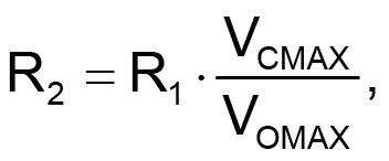
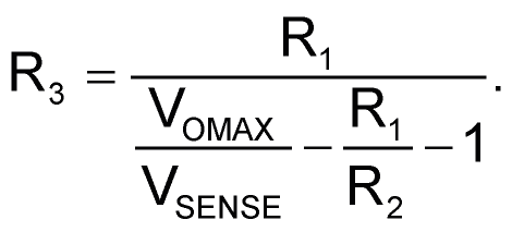
And, in the grand tradition of the KISS principle, that’s it. Ok, ok. Except maybe for a couple of (minor?) caveats. For example:
- Expression 2 above, and therefore the necessary value for R3, must shake out positive. I can’t think of a practical case where it wouldn’t, but there’s probably some perverse permutation of parameters out there where it won’t, and implementing negative resistors isn’t particularly simple.
- The relation between VOUT and VC is inverse. So, the digital version of VC must be 1’s complemented (a totally KISS-bit of software arithmetic to flip all the bits, so 0s become 1s, and 1s become 0s) before being written to the DAC register.
- VIN must be adequate for the chosen chip to generate the chosen VOMAX when VC = 0. Duh.
So maybe it’s not really totally KISS, just mostly.
1) Famous KISS principle: Is a footnote really necessary?