Dwight Byrd and Thomas Kugelstadt, Texas Instruments
Different testing standartds for ESD exist, and which one you use affects your design challenge
ESD (electrostatic discharge) – the sudden and momentary electric current that flows between two objects at different electrical potentials – causes equipment failure and network downtime, thus causing production losses of multiple billions of dollars annually. From portable consumer electronics to industrial-automation, process-control systems, and military and aerospace applications, every electronics manufacturer must consider ESD during equipment design. Myriad testing standards exist for addressing the range of technical requirements of the various industrial segments.
To help you select the correct testing standard for a design, you need to understand the main ESD standards and the differences between device- and system-level testing. ESD protection includes a range of protection schemes, the most common of which are steering-diode arrays, TVS (transient-voltage-suppressor) diodes, and zener diodes. No matter which protection scheme you select, you must perform a final EMI (electromagnetic-interference) test and a test of the protection circuit itself.
HBM testing
The HBM (human-body-model) device-level test is the most common model for ESD testing. It is used to characterize the susceptibility of an electronic component to ESD damage. The test simulates an electrical discharge of a human onto an electronic component, which could occur if a human has built up residual charge – for example, by dragging his feet, in socks, across a carpet and then touching an electronic device. The failure modes for the HBM testing of ICs typically comprise junction damage, metal penetration, melting of metal layers, contact spiking, and damage to the gate oxides.
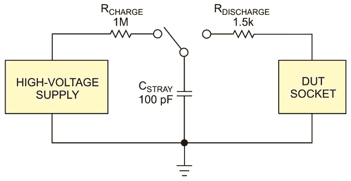
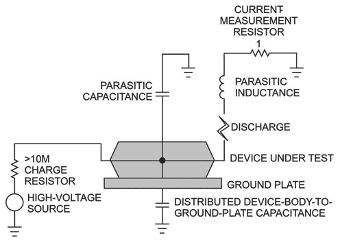
You set up the test procedure by applying a high-voltage supply in series with a 1-MΩ resistor and a 100-pF capacitor. After the capacitor is fully charged, a switch is used to remove it from the high-voltage supply and series resistor and to apply it in series with a 1.5-kΩ resistor and the DUT (device under test). The voltage thus fully dissipates through the resistor and the DUT (Figure 1). Values for the high-voltage supply range, according to the test level, from 0.5 to 15 kV.
 |
|
| Figure 1. | The HBM device-level test is the most common model for ESD testing. You use it to characterize the susceptibility of an electronic component to ESD damage. |
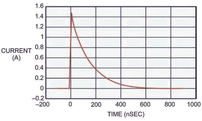
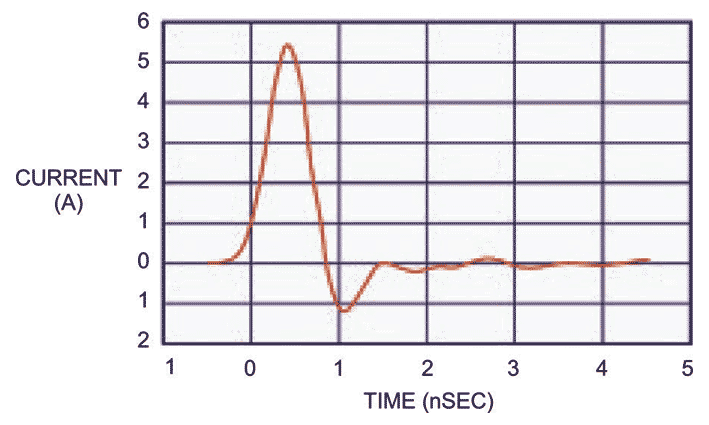
Figure 2 shows a typical oscilloscope readout with an initial current spike as large as 1.4 to 1.5A when the capacitor starts discharging and the ramp-down until it asymptotically approaches 0A at approximately 500 nsec. The DUT can experience a maximum power of 22.5 kW at a single discharge event on a traditional HBM. Keep in mind that power equals the current times the voltage.
 |
|
| Figure 2. | A typical oscilloscope readout shows an initial current spike as large as 1.4 to 1.5A when the capacitor starts discharging and the ramp-down until it asymptotically approaches 0A at approximately 500 nsec. |
MM testing
The MM (machine-model) device-level test, which emerged in the 1990s, is now less common than the HBM test. Industrial-automation-manufacturing sites became increasingly popular in the ’90s to increase output. These machines become electrically charged after turn-on and discharge into an electronic component after making contact. Thus, MM tests became a model for testing this type of ESD event. Failure modes in MM testing are similar to those in HBM testing. These failure modes include junction damage, melting metal layers, and gate-oxide damage.
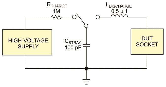
You set up the test procedure for MM testing with a high-voltage supply in series with a resistor and a 200-pF capacitor. After the capacitor fully charges, a switch is used to remove it from the high-voltage supply and series resistor and then apply it in series to a 0.5-μH inductor and the DUT. The inductor with the capacitor voltage dissipates through the DUT (Figure 3). Traditional values for the high-voltage supply can vary, but the most common range is 50 to 400V.
 |
|
| Figure 3. | You set up the test procedure for MM testing with a highvoltage supply in series with a resistor and a 200-pF capacitor. |
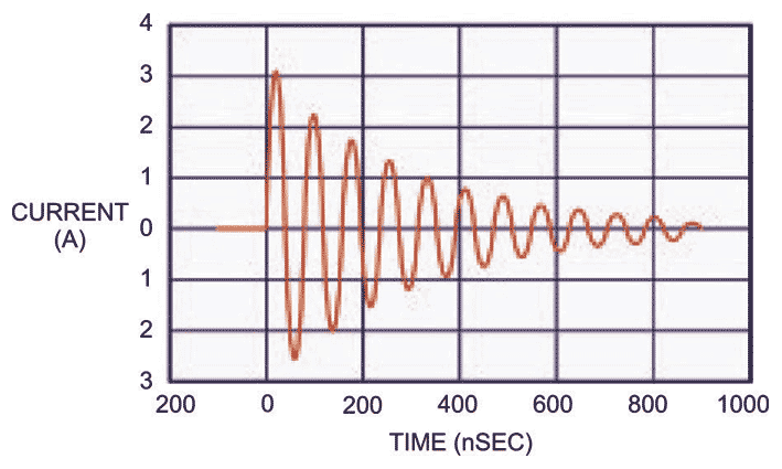
When looking at an oscilloscope measurement of current over time, you can see that the RLC (resistance/inductance/capacitance) circuit creates an alternating current (Figure 4). The current reaches approximately ±3A, which is about four times higher than the HBM’s peak-to-peak current amplitude. Furthermore, the dissipation is much longer for the MM test because it is still asymptotically approaching 0A at 900 nsec (Figure 4). The DUT experiences a maximum power dissipation of approximately 1.2 kW during an discharge event. MM testing requires that you test each pin on the DUT to its standard. The electronic chip is mounted on a specially designed load board that interfaces with an automated ESD tester. You ground the other pins on the board and then individually test each pin. You continue this procedure until all pins have been tested.
 |
|
| Figure 4. | An oscilloscope measurement of current over time shows that the RLC circuit creates an alternating current. |
CDM testing
The CDM (charged-device-model) device-level testing procedure is a simulation for situations that often happen in automated-manufacturing environments in which machines often remain on indefinitely, causing the electronic ICs to electrically charge over time. When the part comes into contact with a grounded conductor, the built-up residual capacitance discharges. For the CDM test, the DUT is placed on its back facing upward on a testing board. Separate the metal field plate and the DUT with an insulating material, which acts as a capacitor between the two objects. You then connect the metal field plate to a high-voltage supply and increase its voltage to the required CDM-test-voltage level. A probe then approaches the pin under test where an ESD event occurs. Monitoring the ground connection of the pin under test verifies this action. Repeat this test on each pin of the DUT for three positive and three negative pulses. The result is six total discharges per pin (Figure 5).
 |
|
| Figure 5. | Separate the metal field plate and the DUT with an insulating material, which acts as a capacitor between the two objects. You then connect the metal field plate to a high-voltage supply and increase its voltage to the required CDM-test-voltage level. |
Figure 6 indicates that the CDM discharge takes place over 2 nsec at most, which makes it difficult to test and to model. This test results in a current of 5 to 6A discharging in less than 1 nsec. The current dissipates within 5 nsec, making this part of the test succinct but volatile. Due to this fast transient, the failure modes typically seen in CDM tests are gate-oxide damage, charge trapping, and junction damage. Figure 6 shows the current waveform during a CDM test. The HBM, MM, and CDM are the most common ESD device-level testing procedures for electronic components. Table 1 summarizes their similarities and differences.
 |
|
| Figure 6. | CDM discharge takes place over 2 nsec at most, which makes it difficult to test and to model. This test results in a current of 5 to 6A discharging in less than 1 nsec. |
| Table 1. Comparison of HBM, MM, and CDM testing. | |||
|
Model
|
HBM
|
MM
|
CDM
|
|
Test levels
|
2, 4, 8, and 15 kV
|
100, 150, and 200V
|
250, 500, 750, and 1000V
|
|
Peak current (A)
|
1.5
|
±3
|
5 to 6
|
|
Pulse width (nsec)
|
Approximately 150
|
Approximately 80
|
Approximately 1
|
|
Rise time
|
2 to 10 nsec
|
Approximately 1 nsec
|
Less than 400 psec
|
|
Typical ESD
failures |
Junction damage,
metal penetration, metal melting, contact spiking, and gate-oxide damage |
Junction damage,
metal melting, and gate-oxide damage |
Gate-oxide damage,
charge trapping, and junction damage |