Reducing low-frequency (1/f) noise generated by an IC voltage reference can prove difficult. In theory, adding a lowpass filter to a reference's output reduces noise. In practice, a lowpass RC filter for suppression of noise frequencies below 10 Hz requires large values of series resistance and shunt capacitance. Unfortunately, a high-value series resistor introduces resistance errors and thermal noise, and a shunt capacitor's leakage resistance forms an unpredictable and unstable shunt path. Together, the two components form a noisy and temperature-dependent voltage divider that directly affects the reference's accuracy and long-term stability. In addition, pc-board surface contaminants can add yet another possible leakage path and error source.
You can stack multiple voltage references in series to reduce their 1/f noise. The references' dc outputs add linearly, and their uncorrelated internal noise sources add geometrically. For example, consider a stack of four voltage references, each comprising a dc reference source, VREF, in series with a random-noise generator, VNOISE. Adding four reference sources produces the following outputs:

and

The original ratio of noise voltage to dc reference voltage thus divides in half.
 |
|
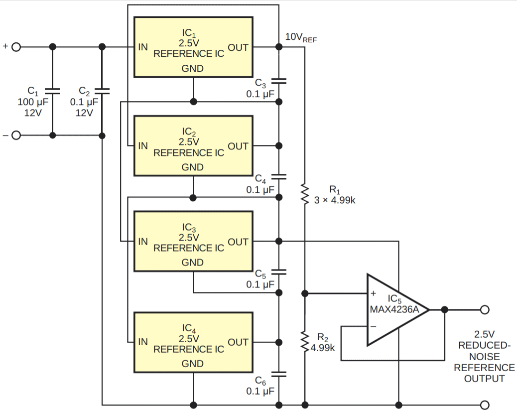
| Figure 1. | Four 2.5 V references, IC1 through IC4, produce 10 V. Resistors R1 and R2 form a voltage divider that reduces the 10 V output to 2.5 V and lowers the output-noise voltage by half. Buffer amplifier IC5 isolates the reference circuit from the load. |
Figure 1 illustrates a method of adding multiple references to produce a single, less noisy reference voltage. The resistors are parts of a highly stable metal-film network, and buffer amplifier IC5 offers low noise, low input-offset voltage, and low offset-temperature coefficients.
| Table 1. | Noise voltages measured in Figure 1 using four 2.5 V MAX6037 voltage references |
||||||||||||||||||
|
|||||||||||||||||||
Table 1 and Table 2 present the noise voltages that result from stacking four each of two types of 2.5 V references. Each table shows the 0.1- to 10-Hz noise voltage for each of the four references, IC1 through IC4, and for the combination. Note that the dispersion in the ratios of rms to peak-to-peak values relates to subjectivity in the method of measuring the values. In addition to lower 0.1- to 10-Hz noise, the circuit also reduces long-term drift of the reference voltage.
| Table 2. | Noise voltages measured in Figure 1 using four 2.5 V MAX6143 voltage references |
||||||||||||||||||
|
|||||||||||||||||||
